semi合集-English.pdf - 第6094页
SEMI G18-96 © SEMI 198 4, 1996 2 7.4 C amber (Edgewise Curvatur e) — C a m b e r i s n o t critical for m aterial used in the etching process provided the en d product (leadfram e strip) m eets it s requirem ents; ± 0.06…
SEMI G18-96 © SEMI 1984, 19961
SEMI G18-96
STANDARD FOR INTEGRATED CIRCUIT LEADFRAME MATERIAL
USED IN THE PRODUCTION OF ETCHED LEADFRAMES
1 Purpose
This specification is for the leadframe material that will
be shipped to an etch house. It is a leadframe
specification, but deals with material aspects only.
2 Scope
This specification covers the special requirements for
metal strip to be used to fabricate integrated circuit
leadframes by etching.
3 Referenced Documents
3.1 ASTM Specifications
1
ASTM B 601 — Recommended Practice for Temper
Designations for Copper and Copper Alloys —
Wrought and Cast
ASTM E 8 — Methods of Tension Testing of Metallic
Materials
ASTM B 193 — Test Method for Resistivity of
Electrical Conductor Materials
ASTM B 754 — Standard Test Method for Measuring
and Recording the Deviations from Flatness in Copper
and Copper Alloy Strip
4 Terminology
None.
5 Ordering Information
5.1 Orders for material under this specification shall
include the following information:
1. Quantity of each size
2. Alloy name and number
3. Temper or mechanical properties
4. Dimensions: Thickness and width (see Section 7.3.)
5. How furnished: Coils and coil size or sheet size (see
Section 10.)
6. Certification or test report requirements (see Section
11.)
1 American Society for Testing and Materials, 100 Barr Harbor
Drive, West Conshohoken, PA 19428-2959
7. Packaging and marking requirements (see Section
12.)
6 General Requirements
6.1 The materials covered by this specification shall
conform to the requirements detailed in this
specification, unless otherwise agreed upon by supplier
and purchaser.
7 Dimension and Tolerance s
7.1 The following tests shall be used to determine
conformance or non-conformance to this specification.
7.2 Etched Raw Materials Purchased in Coils —
Samples can be taken from the ID or OD of each coil. If
the material does not conform to this specification,
remove two wraps from the ID and OD of each coil and
test for conformance again. Samples may also be taken
from cut sheets.
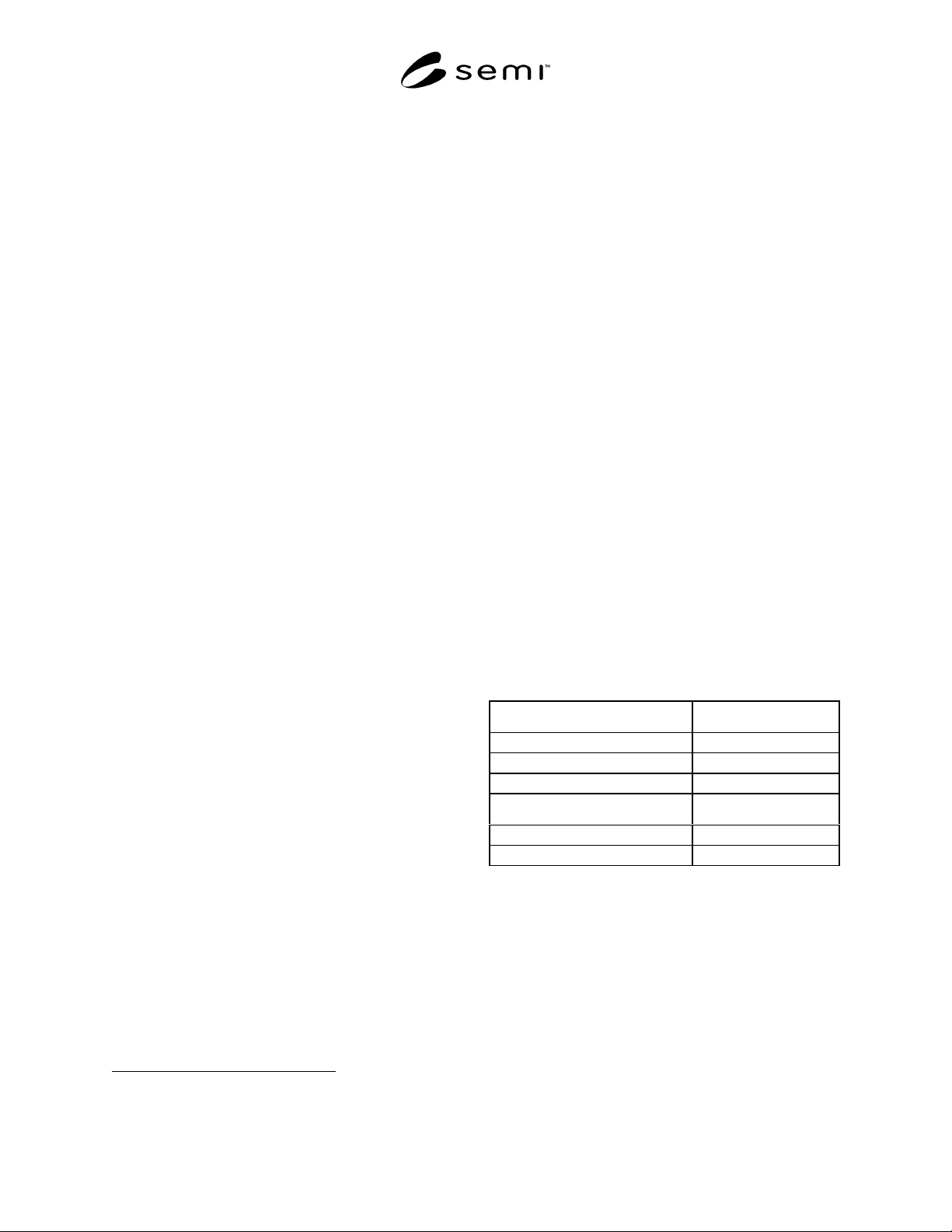
7.3 Thickness, Width, and Length — The tolerances
for thickness and width shall be as shown in Table 1.
More restrictive tolerances than those shown in Table 1
or tolerances for other thicknesses and widths shall be
agreed upon between user and supplier.
Table 1 Thickness and Width Tolerances
Thickness Tolerance
0.005 - 0.010" (0.127 – 0.254 mm) ± 0.0003" (0.008 mm)
0.015" (0.381 mm) ± 0.0004" (0.010 mm)
0.020" (0.508 mm) ± 0.0005" (0.013 mm)
Width Tolerance
2.000 - 8.000" (25.4 - 203.2 mm) ± 0.005" (0.127 mm)
> 8.000" (> 203.2 mm) to ± 0.010" (0.254 mm)
SEMI G18-96 © SEMI 1984, 1996 2
7.4 Camber (Edgewise Curvature) — Camber is not
critical for material used in the etching process
provided the end product (leadframe strip) meets its
requirements; ± 0.0625" (1.6 mm) in 36" (91 cm) is
considered acceptable.
7.5 Coil Set — A three foot long sample shall be
obtained from each coil supplied. The measured coil set
shall not exceed 1.500" (38.1 mm).
7.6 Edge Burrs — Undesirable and, if present, their
height shall not exceed 10% of the metal thickness.
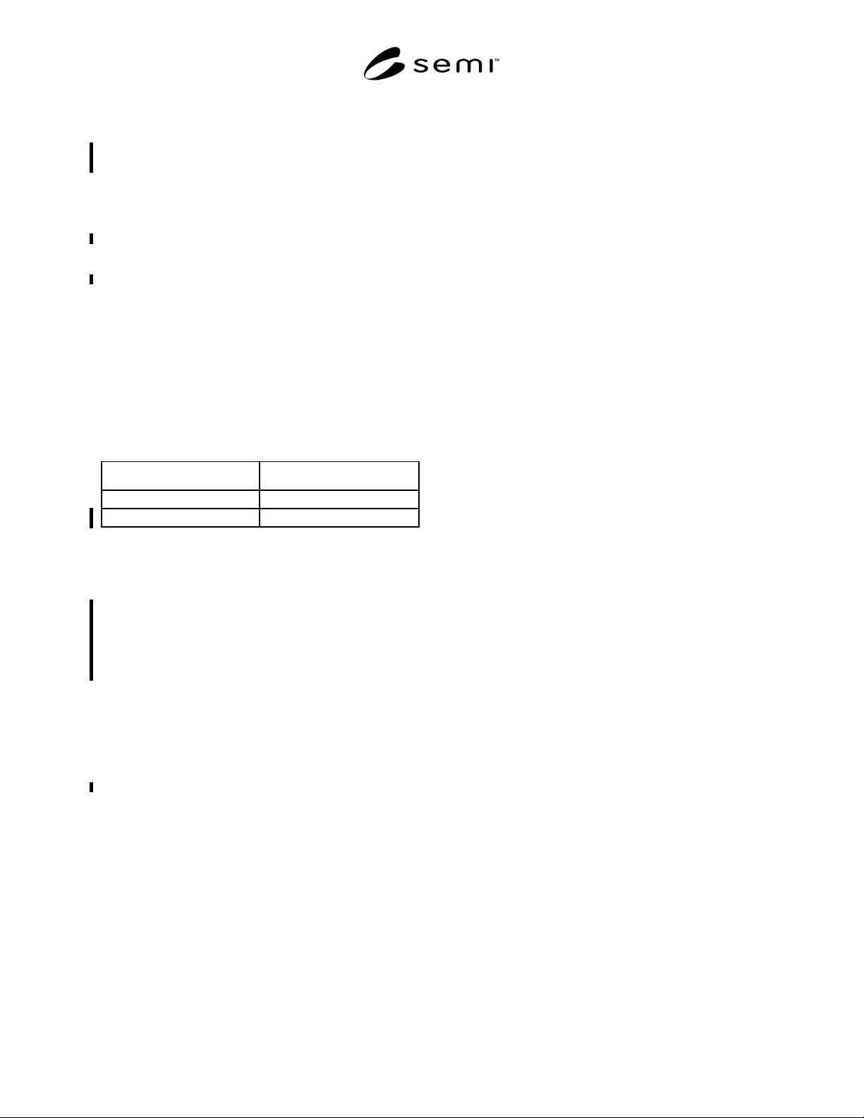
7.7 Crossbow (Dish) — Crossbow is a function of
slitting. Because material for the photo chemical
process is generally about 16–20" wide, crossbow is not
a critical problem. However, the final product
(leadframe strips) must meet maximums, as suggested
in Table 2, and crossbow in the sheet form, shall not be
present to the extent that this specification cannot be
met.
Table 2 Maximum Crossbow
Specified Strip Width Maximum Crossbow
Up to 1.000" (25.4 mm), incl. 0.003" (0.076 mm)
Over 1.000" (25.4 mm) 0.005" (0.127 mm)
7.8 Oil Can — When any part of a sheet is pushed, but
not bent, and it snaps into a different position or plane
other than the original position with no further pressure,
oil canning is present. Oil canning shall not be present
on materials being used in the photo chemical process
(etching) to the extent that the maximum crossbow
specification on the finished product (see Table 2)
cannot be met.
8 Surface Finish
8.1 The material shall be commercially free of surface
imperfections such as pits, nicks, dents, gouges,
scratches, laminations, or inclusions.
8.2 Surface defects less than 0.0003" (0.0076 mm) in
depth will be acceptable unless otherwise agreed upon
between the supplier and purchaser.
APPLICATION NOTE: There is a question regarding the
ability of material suppliers to meet this specification.
Revision of this specification is under review.
9 Corrosion
9.1 Visual inspection shall be used to determine if
objectionable surface oxides are present which would
render the product unusable for the intended
application. Objectionable conditions, if present, should
be reported to the supplier within 60 days after receipt
of the material.
9.2 There shall be no visible rust on the surface of
Alloy 42 material.
10 Coils
10.1 Unless otherwise specified, coils shall be
supplied with an inside diameter that provides for good
packing practice without resulting in excessive coil set.
11 Certifications or Test Rep orts
11.1 Requests for certifications or test reports shall be
made at the time of order entry or contract agreement.
They shall be furnished by the manufacturer within one
week of date of shipment.
11.2 When certifications are required, the following
information shall be supplied as a minimum:
1. Vendor name
2. Purchase order number
3. Vendor order number
4. Alloy name and number
5. Chemical analysis
6. Temper designation (reference only)
7. Tensile strength
8. Elongation percent in 2"
9. Electrical conductivity % IACS (for copper base
alloys only)
11.3 In the event of a disagreement between supplier
and purchaser, an independent test shall be conducted
on the strip to verify the data provided in the
certification.
12 Packaging and Marking
12.1 The material shall be separated by size,
composition, and temper, and prepared for shipment in
such a manner as to ensure acceptance by a common
carrier for transportation at the lowest applicable rate.
12.2 The material shall be suitably packaged to protect
from condensation, contamination, etc., and to afford
protection from the normal hazards of transportation.
12.3 Each shipping unit shall be legibly marked with
the purchase order number, alloy name or number,
temper, size, gross and net weight, and name of the
supplier. The specification number shall be shown
when specified on the purchase order.

SEMI G18-96 © SEMI 1984, 19963
12.4 Any special packaging or shipping requirements
shall be agreed upon between supplier and purchaser at
the time of purchase.
13 Basis for Rejection
13.1 For the purposes of determining conformance
with the requirements prescribed in the specification,
any measured value outside the specified limiting
values shall be cause for rejection.
13.2 If objectionable material is found and rejected,
samples of the questionable material, with the defects
identified and marked, should be sent to the supplier
along with information as to order number, quantity
originally received, date received, and quantity rejected.
Rejected material should be held with adequate
protection and identification by the purchaser for a
reasonable amount of time, pending investigation by the
supplier.
NOTICE: These standards do not purport to address
safety issues, if any, associated with their use. It is the
responsibility of the user of these standards to establish
appropriate safety and health practices and determine
the applicability of regulatory limitations prior to use.
SEMI makes no warranties or representations as to the
suitability of the standards set forth herein for any
particular application. The determination of the
suitability of the standard is solely the responsibility of
the user. Users are cautioned to refer to manufacturer’s
instructions, product labels, product data sheets, and
other relevant literature respecting any materials
mentioned herein. These standards are subject to
change without notice.
The user’s attention is called to the possibility that
compliance with this standard may require use of
copyrighted material or of an invention covered by
patent rights. By publication of this standard, SEMI
takes no position respecting the validity of any patent
rights or copyrights asserted in connection with any
item mentioned in this standard. Users of this standard
are expressly advised that determination of any such
patent rights or copyrights, and the risk of infringement
of such rights, are entirely their own responsibility.
Copyright by SEMI® (Semiconductor Equipment and Materials
International), 3081 Zanker Road, San Jose, CA 95134. Reproduction o
f
the contents in whole or in part is forbidden without express written
consent of SEMI.