semi合集-English.pdf - 第5877页
SEMI P36-0600 © SEMI 2000 4 marker made on s pecim en stage AB spec imen sta ge wafer AB Cros s sec tion ≈ 4.8** M3 or M4** chip-type magnification reference chip-type magnification referenc e **Recommende d value Figure…
SEMI P36-0600 © SEMI 20003
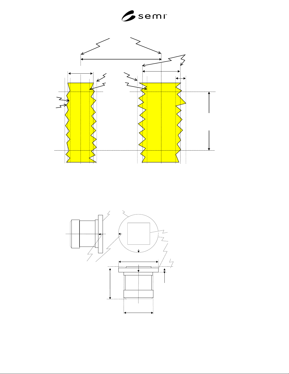
center-to-center pitch
centerline
pattern edge mean line
or
least squares best fit line
linewidth
peak-to-peak edge
roughness
defined measurement length
segment
linewidth
peak line
valley line
peak
valley
NOTE 1: The figure ignores that fact that the SEM image is gray-scale and not black and white. Use the same intensity threshold
setting for measuring pitch as for line width The center-to-center pitch averaged over the measurement length segment is to be
certified and used for SEM magnification calibration
Figure 1
Definition of Edge Roughness
chip
stub
chip surface*
φ15
≈10.5
1.7±0.05
−0.032
−0.050
marker
stub
≈
φ
17
* The flatness of the chip
surface to the specimen stage
surface could be automatically
determined by setting the
magnification reference on the
specimen stage.
Figure 2
Shape and size of chip-type magnification reference: unit mm
SEMI P36-0600 © SEMI 2000 4
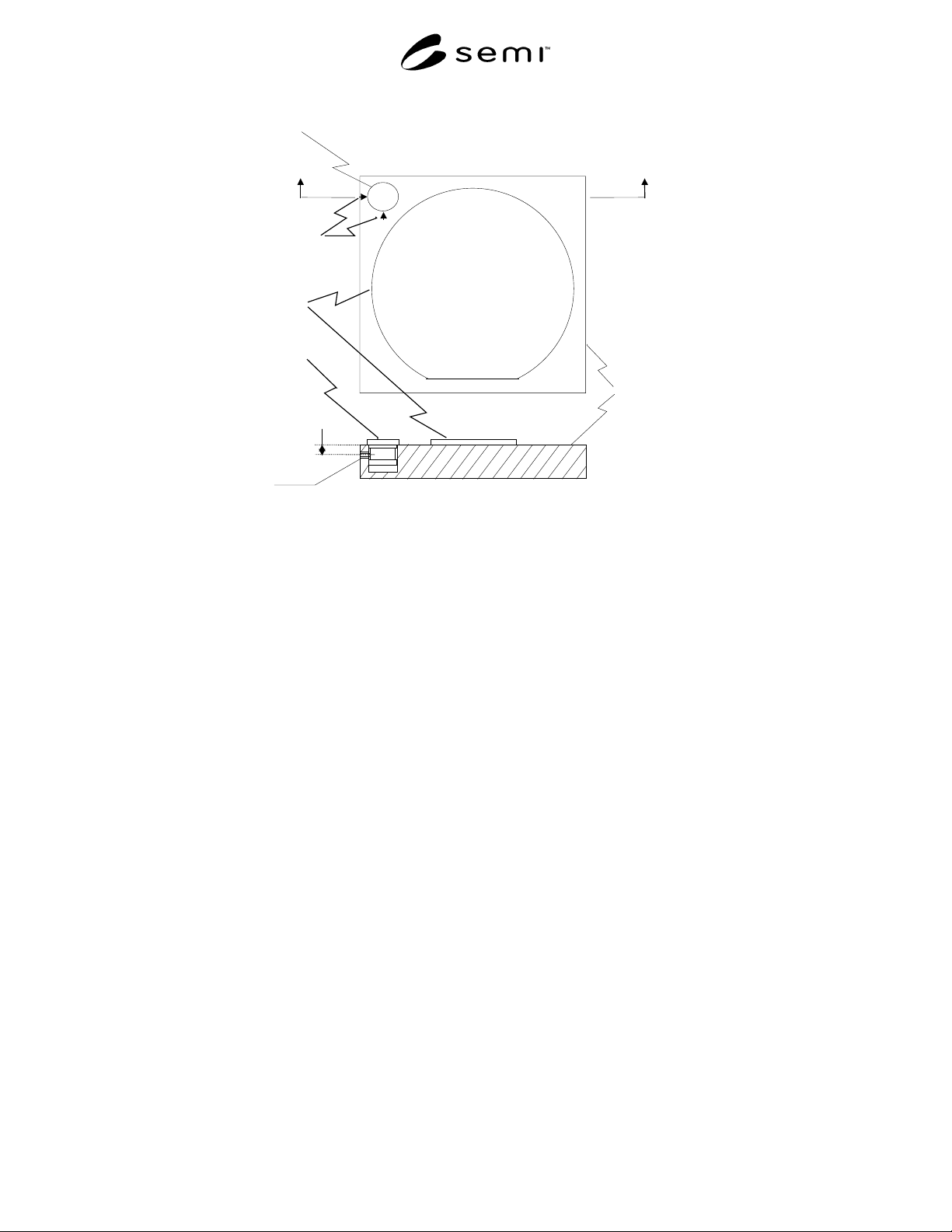
marker made
on specimen
stage
AB
specimen stage
wafer
AB Cross section
≈
4.8**
M3 or M4**
chip-type magnification reference
chip-type
magnification
reference
**Recommended value
Figure 3
Chip-type magnification reference mounted on specimen stage: unit mm

SEMI P36-0600 © SEMI 20005
APPENDIX 1
NOTES
NOTE: The material in this appendix is an official part of
SEMI P36 and was approved by full letter ballot procedures
on March 1, 2000 by the Japanese Regional Standards
Committee.
A1-1 Reference patterns for adjusting CD-SEM
magnification using their pitches and reference patterns
for optimizing pattern-edge determination parameters
using their widths
A1-2 The following procedures are generally applied
to critical dimension measurements using CD-SEMs: an
electron beam linearly scans across the measured
pattern, secondary and/or reflected electrons emitted
from every electron-beam incident point are collected
to form its intensity profile, pattern edges are
determined on the intensity profile using a designated
pattern-edge determination method, and the measure-
ment value of the width of the pattern is obtained from
the distance between the two pattern edges.
A1-3 Therefore, measurement errors of CD-SEM
measurements can be partitioned into two components:
one is magnification error and another is pattern-edge
determination error. Magnification error is caused by
variation of the equipment conditions such as the
sampling pitch and incident angle of electron beam.
Pattern-edge determination error is affected by the
manner of measurement such as pattern-edge
determination algorithm used and pattern-edge
determination parameters used, and the properties of the
specimen such as pattern topography (e.g., pattern-edge
slope) and pattern material.
A1-4 Magnification error, including inter-machine
magnification error, can be detected and corrected
through measuring pitches of reference patterns, and
pattern-edge determination error could be detected and
corrected through measuring widths of the reference
patterns practical reference patterns are available for
measuring their widths. However, it seems extremely
difficult to produce practical reference patterns for
measuring their widths; the source of the problem lies
in the physics of electron beam image formation and
not because the reference patterns are somehow
inadequate because of the following reasons: (a)
reference pattern can not be determined uniquely, since
intensity profiles obtained are different from each other
dependent on pattern topography and pattern materials
even if the width of every reference pattern is the same,
(b) it is technologically difficult to solve the problem of
width change due to the contamination which changes
the measurement value of pattern width dependent on
measurement time.
NOTICE: SEMI makes no warranties or
representations as to the suitability of the guideline set
forth herein for any particular application. The
determination of the suitability of the guideline is solely
the responsibility of the user. Users are cautioned to
refer to manufacturer’s instructions, product labels,
product data sheets, and other relevant literature
respecting any materials mentioned herein. These
guidelines are subject to change without notice.
The user’s attention is called to the possibility that
compliance with this guideline may require use of
copyrighted material or of an invention covered by
patent rights. By publication of this guideline, SEMI
takes no position respecting the validity of any patent
rights or copyrights asserted in connection with any
item mentioned in this guideline. Users of this
guideline are expressly advised that determination of
any such patent rights or copyrights, and the risk of
infringement of such rights, are entirely their own
responsibility.
Copyright by SEMI® (Semiconductor Equipment and Materials
International), 3081 Zanker Road, San Jose, CA 95134. Reproduction o
f
the contents in whole or in part is forbidden without express written
consent of SEMI.