semi合集-English.pdf - 第5777页
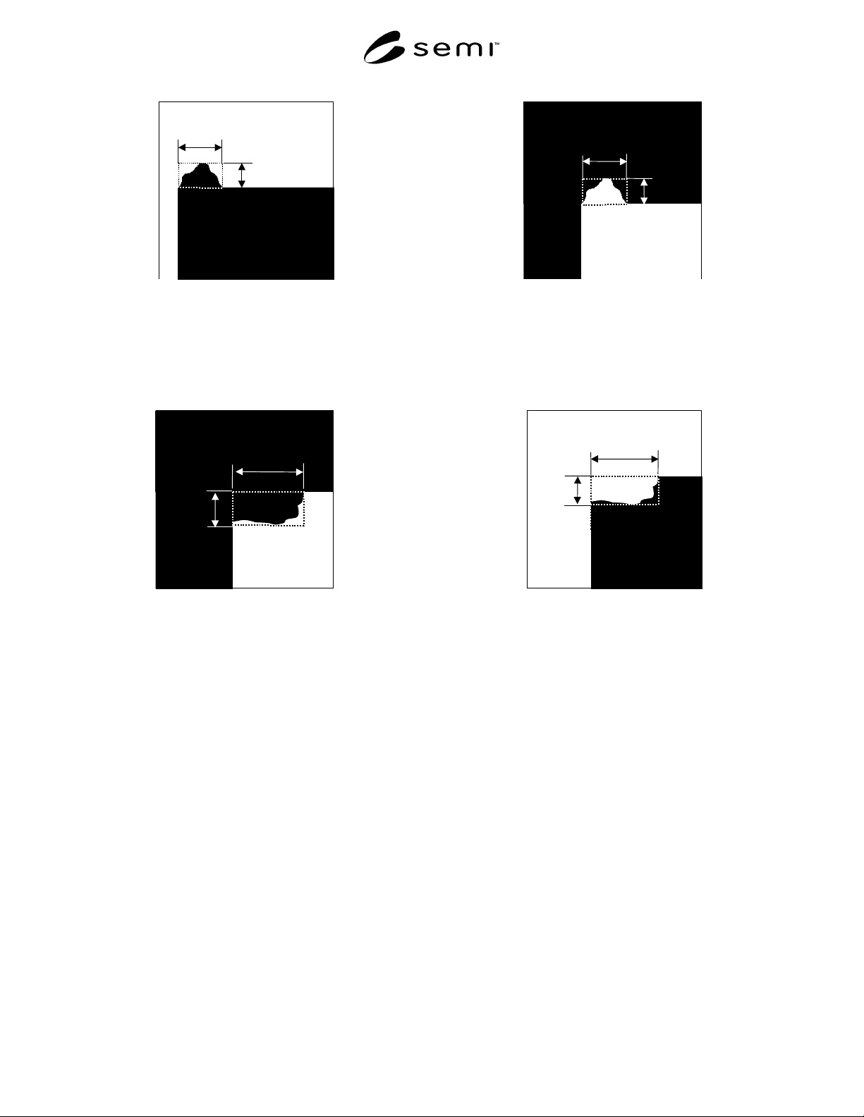
SEMI P22-0699 © SEMI 1993 , 1999 7 S2 S1 S2 S1 Figure 27 Figure 28 Corner Extensio n Randomly S haped Corner Int rusion Rando mly Shaped S1 S2 S2 S1 Figure 29 Figure 30 Corner Extensio n Randomly S haped Corner Int rusio…
SEMI P22-0699 © SEMI 1993, 1999 6
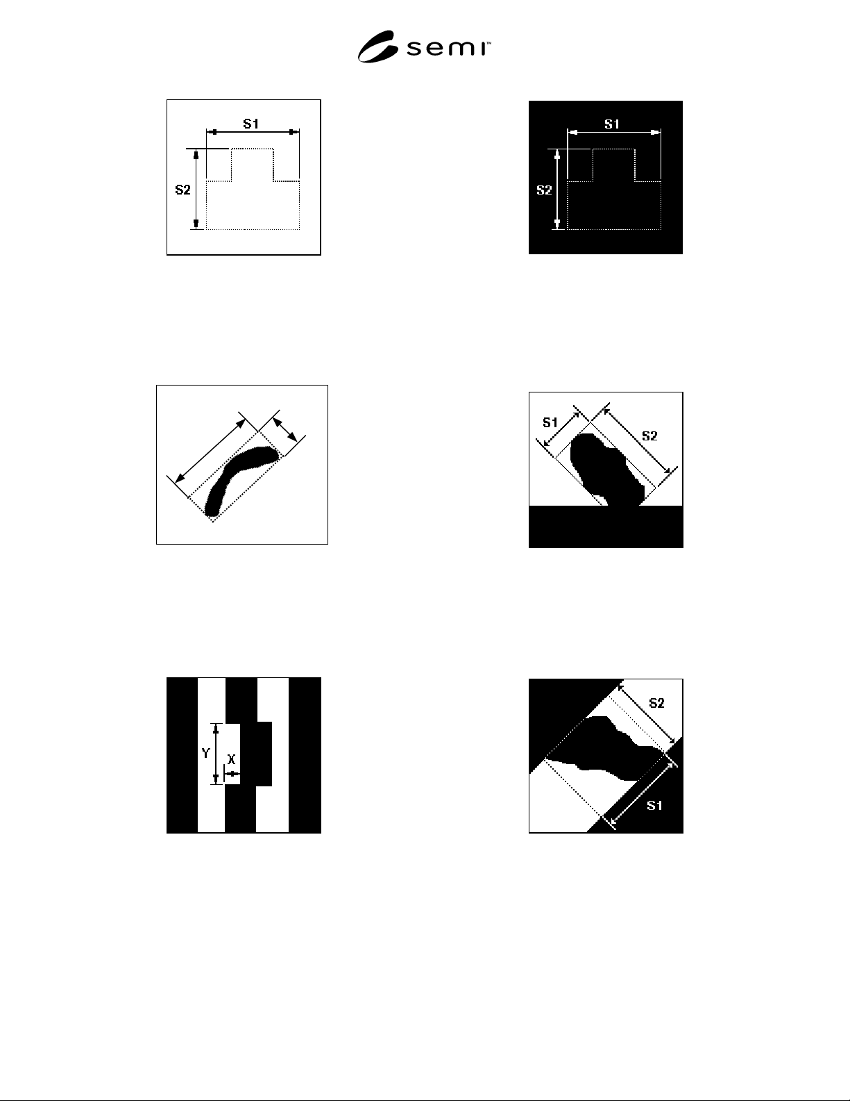
Figure 21 Figure 22
Missing Opaque Pattern Missing Clear Pattern
S1
S2
Figure 23 Figure 24
Dot Randomly Shaped Edge Extension Randomly Shaped
Figure 25 Figure 26
Misplacement On Opaque Pattern Opaque Bridge
SEMI P22-0699 © SEMI 1993, 19997
S2
S1
S2
S1
Figure 27 Figure 28
Corner Extension Randomly Shaped Corner Intrusion Randomly Shaped
S1
S2
S2
S1
Figure 29 Figure 30
Corner Extension Randomly Shaped Corner Intrusion Randomly Shaped
NOTICE: These standards do not purport to address
safety issues, if any, associated with their use. It is the
responsibility of the user of these standards to establish
appropriate safety and health practices and determine
the applicability of regulatory limitations prior to use.
SEMI makes no warranties or representations as to the
suitability of the standards set forth herein for any
particular application. The determination of the
suitability of the standard is solely the responsibility of
the user. Users are cautioned to refer to manufacturer's
instructions, product labels, product data sheets, and
other relevant literature respecting any materials
mentioned herein. These standards are subject to
change without notice.
The user's attention is called to the possibility that
compliance with this standard may require use of
copyrighted material or of an invention covered by
patent rights. By publication of this standard, SEMI
takes no position respecting the validity of any patent
rights or copyrights asserted in connection with any
item mentioned in this standard. Users of this standard
are expressly advised that determination of any such
patent rights or copyrights, and the risk of infringement
of such rights are entirely their own responsibility.
Copyright by SEMI® (Semiconductor Equipment and Materials
International), 3081 Zanker Road, San Jose, CA 95134. Reproduction o
f
the contents in whole or in part is forbidden without express written
consent of SEMI.

SEMI P23-0200 © SEMI 1993, 20001
SEMI P23-0200
GUIDELINES FOR PROGRAMMED DEFECT MASKS AND
BENCHMARK PROCEDURES FOR SENSITIVITY ANALYSIS OF MASK
DEFECT INSPECTION SYSTEMS
These guidelines were technically approved by the Global Mask and Mask Equipment Committee and are the
direct responsibility of the Japanese Mask and Mask Equipment Committee. Current edition approved by the
Japanese Regional Standards Committee on September 10, 1999. Initially available at www.semi.org
February 2000; to be published February 2000. Originally published in 1993; previously published in 1996.
NOTE: These guidelines were rewritten in their entirety
in February 2000.
1 Purpose
1.1 The purpose of this guideline is to propose a test
mask to be used for evaluation of the sensitivity of
Mask Defect Inspection Systems. This test mask
consists of test chips including programmed pattern
defects and reference test chips without programmed
defects. Since the test chip is an assembly of cells, the
test chips are defined in this guideline by cell patterns,
programmed defects in cell patterns, and the layout of
the cells. Also, the test mask is defined by defining the
test chips arrangement. Furthermore, the use of this
mask is described. It is desirable that these test masks
and benchmark procedures be used when the sensitivity
of a Mask Defect Inspection System is evaluated.
1.2 Background — Different masks have been used by
many equipment manufacturers and users in the past,
and sensitivity has been tested by various methods
decided independently by each manufacturer and user.
In some cases, no common measurement methods or
sensitivity analysis methods have been agreed upon.
Therefore, confusion exists concerning the sensitivity
comparison of equipment between manufacturers, the
definition for specifications between users and
suppliers, and the definition for specifications between
users. Also, due to the fact that several problems were
found when using the previous guideline in actual
manufacturing, the document has been reviewed and
content has been changed throughout. It was also the
goal of this revision, while considering ease of
manufacturing of test masks first, to fully cover the
evaluation of mask defect inspection systems.
2 Scope
2.1 This guideline defines the content and methods for
use of test masks used in the evaluation of mask defect
inspection systems. Although it is possible to use this
test mask to evaluate transcription of defects etc., this
standard does not attempt to define these processes.
2.2 This guideline shall be revised when a new
effective measurement technology for defect sizing
becomes commonly available in the market.
2.3 This guideline does not purport to address safety
issues, if any, associated with its use. It is the
responsibility of the users of this guideline to establish
appropriate safety and health practices and determine
the applicability of regulatory limitations prior to use.
3 Referenced Standards
3.1 SEMI Standards
SEMI P1 Specification for Hard Surface Photomask
Substrates
SEMI P22 Guideline for Photomask Defect
Classification and Size Definition.
SEMI P33 Provisional Specification for
Developmental 230 mm Square Hard Surface
Photomask Substrates
NOTE 1: As listed or revised, all documents cited shall be the
latest publications of adopted standards.
4 Terminology
4.1 Definitions
4.1.1 Many terms relating to photomask technology
are defined in SEMI P22 and SEMI P33.
4.1.2 design pattern pattern of intended design
data.
4.1.3 photomask pattern pattern on photomask
surface.
5 Mask (See Figure 1)
5.1 Masks will be either 5" or 6" which meet SEMI
P1; both the 5" and 6" will be the same layout.
5.2 Masks will be limited to two types, namely
Conventional and Attenuated (Half Tone). Note that
Levenson and Optical Proximity Correction (OPC)
types will not be included.