semi合集-English.pdf - 第5455页
SEMI M61-0705 © SEMI 2005 4 6.3.4 The pattern step height A as shown in Figure 3, shall meet the nominal value X within th e tolerance Y , as specified in nanometers (nm ). Figure 3 Cross-Sectional View of Epitaxial Su…
SEMI M61-0705 © SEMI 2005 3
ITEM SPECIFICATION
6 Requirements
6.1 General Characteristics
6.1.1 The epitaxial wafers with buried layers shall meet all requirements specified in the purchase order including
those requirements related to both the substrate wafer and epitaxial layer properties.
6.2 Photolithography Characteristics
6.2.1 The identified mask shall be used in making the pattern for the diffused layers.
6.2.2 The alignment precision shall meet the specified requirements as follows:
6.2.2.1 The values of X and Y, the displacement of the center of the pattern from a reference position defined in the
wafer specification in terms of the wafer coordinate system defined in SEMI M20, shall not exceed the maximum
values specified.
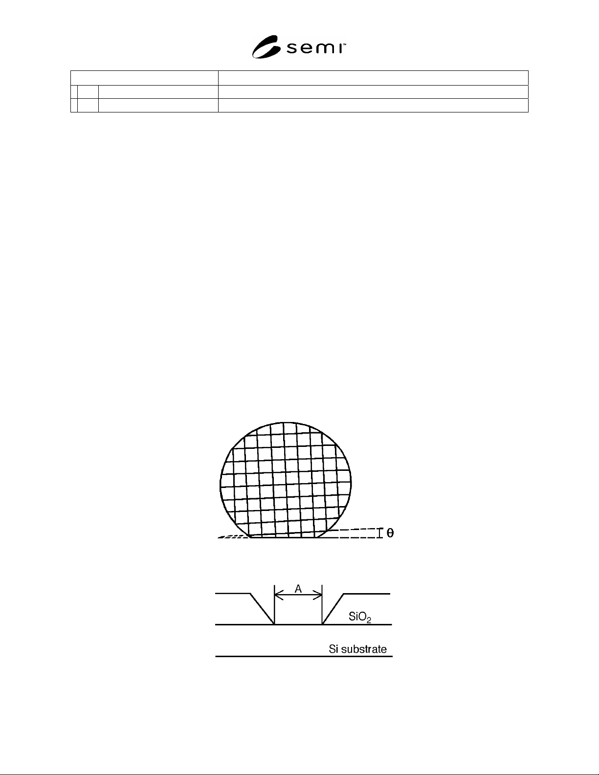
6.2.2.2 The value of θ, the angle between the x-axis of the pattern and the primary orientation flat (see Figure 1)
shall not exceed the maximum value specified.
6.2.3 The pattern line widths (see Figure 2) shall be within the specified tolerance of the desired values.
6.3 Buried Layer Characteristics
6.3.1 The dopant shall be the element specified: boron (B), phosphorus (P), antimony (Sb) or arsenic (As).
6.3.2 The diffusion depth shall fall within the tolerance of the nominal value specified in micrometers (m).
6.3.3 The sheet resistance of the diffused layer shall fall within the tolerance of the value specified in ohms per
square (/sq).
Figure 1
First Mask Showing Angular Displacement
Figure 2
Schematic Diagram Showing Line Width, A, of Pattern on Substrate Wafer
SEMI M61-0705 © SEMI 2005 4
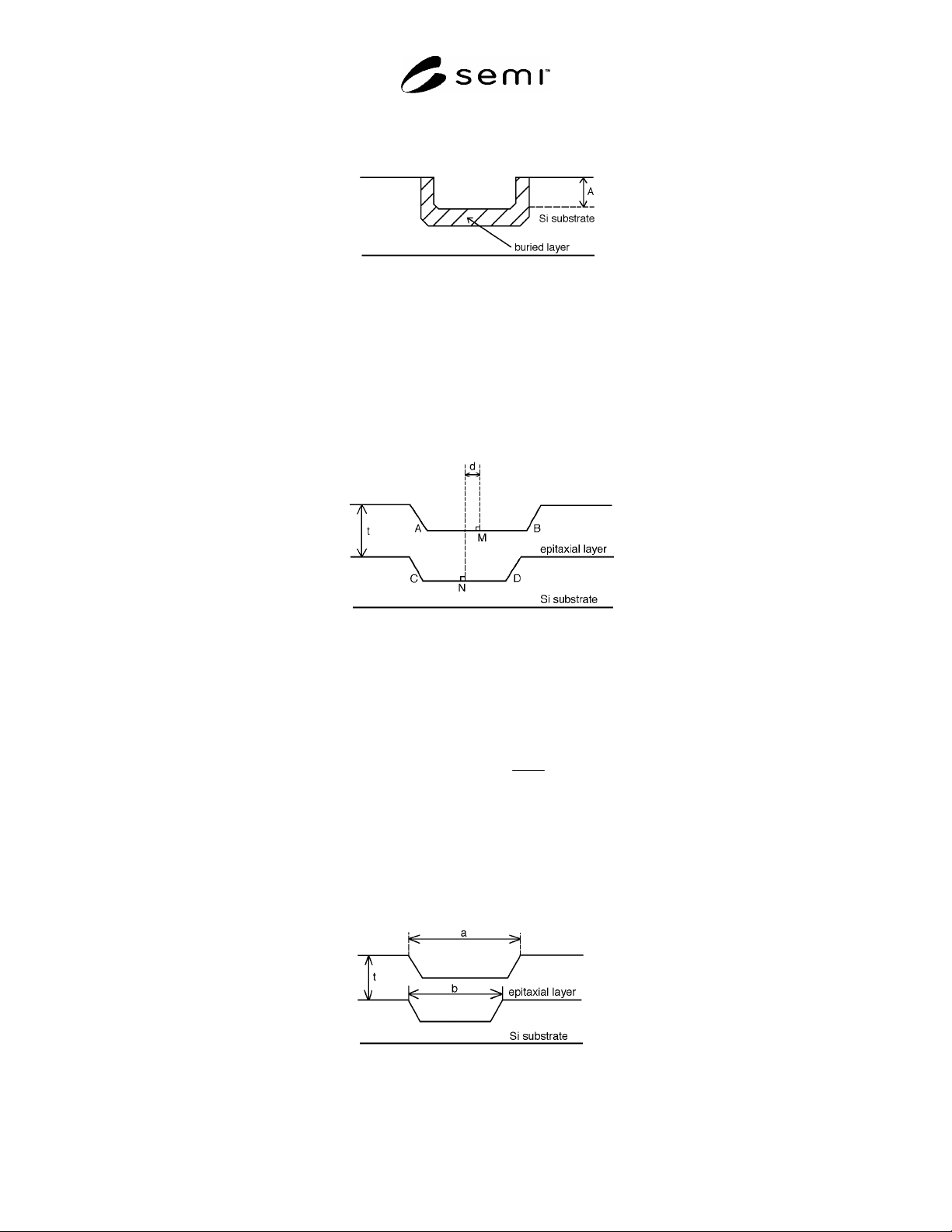
6.3.4 The pattern step height A as shown in Figure 3, shall meet the nominal value X within the tolerance Y, as
specified in nanometers (nm).
Figure 3
Cross-Sectional View of Epitaxial Substrate After Oxide Removal but Before Deposition of the Epitaxial Layer
Showing the Pattern Step Height, A
6.3.5 The defect density on the surface after deposition but before growth of the epitaxial layer shall not exceed the
density specified in number of defects per square centimeter.
6.4 Buried Layer Pattern Characteristics after Growth of the Epitaxial Layer
6.4.1 The pattern shift ratio d/t (see Figure 4) shall meet the specified requirements for nominal value X and
tolerance ±Y, both of which are dimensionless because both d and t are in micrometers (µm).
Figure 4
Cross-Section View of Epitaxial Wafer Showing the Pattern Shift, d.
Not to scale: AM = MB and CN = ND
6.4.2 The pattern distortion ratio shall not exceed the maximum value specified. This dimensionless ratio is equal
to
t
ba
ratio distortionpattern (1)
where:
a = width of pattern on epitaxial layer,
b = width of pattern on substrate, and
t = thickness of epitaxial layer
as shown in Figure 5
Figure 5
Cross-Section View of Epitaxial Layer Showing the Pattern Widths, a,
at the Epi Surface, and b, at the Layer-Substrate Interface

SEMI M61-0705 © SEMI 2005 5
6.5 Wafers shall meet all requirements related to other characteristics, if any such requirements are specified in the
purchase order.
7 Sampling
7.1 Unless otherwise specified, appropriate sample sizes shall be selected from each lot in accordance with
ANSI/ASQC Z1.4. Each quality characteristic shall be assigned an acceptable quality level (AQL) or lot tolerance
percent defective (LTPD) value in accordance with ANSI/ASQC Z1.4 definitions for critical, major, and minor
classifications. If desired and so specified in the contract or order, each of these classifications may alternatively be
assigned cumulative AQL or LTPD values. Inspection levels shall be agreed upon between the supplier and the
customer.
8 Test Methods
8.1 Because no test methods have been standardized and identified in Table 1, all tests to be made to assure that the
wafers meet the required characteristics shall be agreed upon between supplier and customer.
9 Certification
9.1 Upon request of the customer in the contract or order, a manufacturer’s or supplier’s certification that the
material was manufactured and tested in accordance with this specification, together with a report of the test results,
shall be furnished at the time of shipment.
9.2 In the interest of controlling inspection costs, the supplier and the customer may agree that the material shall be
certified as “capable of meeting” certain requirements. In this context, “capable of meeting” shall signify that the
supplier is not required to perform the appropriate tests. However, if the customer performs the test and the material
fails to meet the requirement, the material may be subject to rejection.
10 Product Labeling
10.1 The wafers supplied under these specifications shall be identified by appropriately labeling the outside of each
box or other container and each subdivision thereof in which it may reasonably be expected that the wafers will be
stored prior to further processing. Identification shall include as a minimum the nominal diameter, conductivity
type, dopant, orientation, resistivity range, and lot number. The lot number, either (1) assigned by the original
manufacturer of the wafers, or (2) assigned subsequent to wafer manufacture but providing reference to the original
lot number, shall provide easy access to information concerning the fabrication history of the particular wafers in
that lot. Such information shall be retained on file at the manufacturer’s facility for at least one month after that
particular lot has been accepted by the customer.
11 Packing
11.1 Special packing requirements shall be subject to agreement between the supplier and customer. Otherwise, all
wafers shall be handled, inspected, and packed in such a manner as to avoid chipping, scratches, and contamination
and in accordance with the best industry practices to provide ample protection against damage during shipment.
NOTICE: SEMI makes no warranties or representations as to the suitability of the standards set forth herein for any
particular application. The determination of the suitability of the standard is solely the responsibility of the user.
Users are cautioned to refer to manufacturer's instructions, product labels, product data sheets, and other relevant
literature, respecting any materials or equipment mentioned herein. These standards are subject to change without
notice.
By publication of this standard, Semiconductor Equipment and Materials International (SEMI) takes no position
respecting the validity of any patent rights or copyrights asserted in connection with any items mentioned in this
standard. Users of this standard are expressly advised that determination of any such patent rights or copyrights, and
the risk of infringement of such rights are entirely their own responsibility.
Copyright by SEMI® (Semiconductor Equipment and Materials
International), 3081 Zanker Road, San Jose, CA 95134. Reproduction of
the contents in whole or in part is forbidden without express written
consent of SEMI.