semi合集-English.pdf - 第4941页
SEMI M10-1296 © SE MI 1987, 1996 1 SEMI M10-1296 STANDARD NOME NCLATURE FOR IDENTIFIC A TION OF STRUCTURES AND FEATURES SEEN ON GALLIUM A RSENIDE WA FERS 1 Scope 1.1 The purpose of this document i s to list, illustrate, …
SEMI M9.7-0200 © SEMI 1995, 2000 6
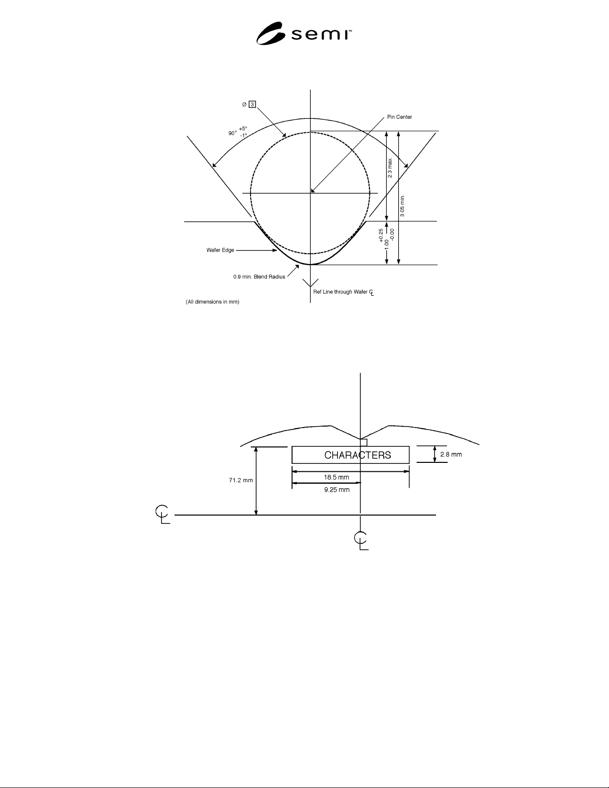
Figure 5
Notch Dimensions
Figure 6
Character Window Location
NOTICE: SEMI makes no warranties or representations as to the suitability of the standards set forth herein for
any particular application. The determination of the suitability of the standard is solely the responsibility of the user.
Users are cautioned to refer to manufacturer’s instructions, product labels, product data sheets, and other relevant
literature respecting any materials mentioned herein. These standards are subject to change without notice.
The user’s attention is called to the possibility that compliance with this standard may require use of copyrighted
material or of an invention covered by patent rights. By publication of this standard, SEMI takes no position
respecting the validity of any patent rights or copyrights asserted in connection with any item mentioned in this
standard. Users of this standard are expressly advised that determination of any such patent rights or copyrights, and
the risk of infringement of such rights, are entirely their own responsibility.
Copyright by SEMI® (Semiconductor Equipment and Materials
International), 3081 Zanker Road, San Jose, CA 95134. Reproduction o
f
the contents in whole or in part is forbidden without express written
consent of SEMI.
SEMI M10-1296 © SEMI 1987, 19961
SEMI M10-1296
STANDARD NOMENCLATURE FOR IDENTIFICATION OF
STRUCTURES AND FEATURES SEEN ON GALLIUM ARSENIDE
WAFERS
1 Scope
1.1 The purpose of this document is to list, illustrate,
and define various characters, features, and
contaminants that are seen on highly polished GaAs
wafers and present recommended practices for
observation of these defects. These occurrences are
frequently referred to as surface defects. The defects
and common synonyms are arranged alphabetically in
Section 4, and each structure is referred to by its most
common name and, in some cases, probably origins.
1.2 Two cases of surface preparations are considered
in this document: (1) surfaces after chemical polishing,
and (2) mechanically and chemically polished surfaces.
1.3 This standard may involve hazardous materials,
operations, and equipment. This standard does not
purport to address all the safety problems associated
with its use. It is the responsibility of whoever uses this
standard to consult and establish appropriate safety and
health practices and determine the applicability of
regulatory limitations prior to use.
2 Applicable Documents
2.1 SEMI Standard
SEMI M9 — Specifications for Round Polished
Monocrystalline Gallium Arsenide Slices
2.2 ASTM Standard
1
F 47 — Crystallographic Perfection of Silicon by
Preferential Etch Techniques
2.3 Other Standard
2
ANSI/ASQC Z1.4-1993 — Sampling Procedures and
Tables for Inspection by Attributes
3 Significance and Use
3.1 This document contains a compilation of the most
commonly observed singularly discernable structures
on polished GaAs surfaces. Ambiguities and
uncertainties regarding surface defects may be resolved
by reference to this document.
1 American Society for Testing and Materials, 100 Barr Harbor
Drive, West Conshohoken, PA 19428-2959 (The cited standard may
be found in Volume 10.05 of the Annual Book of ASTM Standards.)
2 American Society for Quality Control, 611 East Wisconsin Avenue,
Milwaukee, WI 53202
4 Definitions and Descriptions of Terms
cell structure — (block structure): Malformations
attributable to crystal inhomogeneities and that have
their origins in the crystal growth process.
chips — (edge chips, peripheral chips, peripheral
indents, surface chips): Areas of material mechanically
removed from the surface or edge of a wafer.
Chips indicate crystallographic damage in the
adjacent material. The origins of some chips are in
the handling of wafers arising from the physical
transfer or placement of the specimen for process,
measurement, or inspection purposes. The size of a
chip is defined by its maximum radial depth and
peripheral chord length as measurable on an
orthographic shadow projection of the specimen
outline.
apex chip —Any material missing from the edge of a
wafer having at least 2 distinct interior boundaries
which form one or more distinct intersections.
chuck marks — Any physical mark on either surface of
a wafer caused by a chuck or wand.
contaminant — (solvent residue, wax residue, film,
mottled surface, smudge): Surface feature that cannot
be removed by the pre-inspection (non-etching)
cleaning.
NOTE Contaminant may be foreign matter on the surface
such as localized areas which are smudged, stained,
discolored, mottled, etc., or larger areas exhibiting a hazy or
cloudy appearance resulting from a film of foreign material.
Solvent residue: type of film found on wafer
surfaces after solvent evaporation from the surface.
Note: The residue comes from either the solvent
itself or material that the solvent has removed from
the surface and redeposited. Wax residue: film of
wax that migrated onto the wafer surface from
several possible sources.
NOTE The wax originally may have been used to hold the
crystal in place during slicing or polishing. Excessive heat
used in mounting or demounting, during lapping or polishing
processes, may cause the wax to polymerize.
crack — Cleavage or fracture that extends to the surface
of a slice. It may or may not pass through the entire

SEMI M10-1296 © SEMI 1987, 1996 2
thickness of the slice. Often cracks are caused by the
improper handling of wafers.
NOTE Some crack-defect structures can be traced to process
related events.
cavity — (void) A vacancy or hole in the wafer.
NOTE Usually left by dissolved precipitates and Ga
inclusions, As disassociation or created by excess vapor
pressure.
Dimple — Deformation appearing in mechanically
polished GaAs wafers.
NOTE This surface texture can be induced by floating the
wafers during the initial stages of polishing.
Dislocation — See slip, lineage, pit.
edge chip — See chip.
Embedded — abrasive grains Abrasive particles
mechanically forced into the surface of the wafer.
etch pi t — See pit.
film — See contaminant.
flake — Material missing from one, but not the other,
side of a wafer, whose sole interior boundary is one
distinct line or arc not exceeding 2 mm in length, nor
projecting into the wafer beyond the specified edge
exclusion.
gallium inclusion — A segregated Ga-rich droplet
incorporated into the surface structure.
NOTE Normally caused by insufficient As vapor pressure at
the termination of the crystal growth process or by Ga
complexing with some dopants near saturation.
grain boundary — See lineage.
haze — (cloud, nebula): Attributable to light scattering
by concentrations of microscopic surface irregularities
such as pits, oxides, small ridges or scratches, particles,
etc. The light reflection from an individual irregularity
probably could not be readily detected by the unaided
eye, so haze is a mass effect. It is seen as a high density
of tiny reflections.
NOTE This type of contamination may occur during slicing,
lapping, or polishing.
lamella — A special case of the twin. A multiple twin,
extremely thin and relatively long, which may intersect
more than one plane.
lineage — (dislocation pits, grain boundary): Low-
angle grain boundary resulting from an array of
dislocations. This angle may vary from a fraction of a
second to a minute of arc difference in orientation from
one part of the crystal to another. The array of
dislocations will appear as rows of pits on a
preferentially etched surface.
NOTE Lineage can be induced into the material in crystal
growth or in subsequent thermal or epitaxial processes.
Lineage will be visible to the unaided eye only after
preferential etching.
macroscratch —See scratch.
microscratch — See scratch.
microtwin — See twin.
orange peel — (roughness, texture): Large featured
roughened type of surface visible to the unaided eye,
occasionally seen on all types of polished wafers.
NOTE Orange peel is usually symptomatic of a process
control problem. In the case of chemical polishing for
instance, an excessively fast polishing rate, or nonuniform
flow of oxidizer during polishing, can result in orange peel.
Conversely, it can also be caused by insufficient stock
removal.
particulate — (dust): Discrete particle of material
which can usually be removed by (non-etching)
cleaning.
pit — (dislocation, etch pit): Depression in the wafer
surface which has a definite and distinguishable shape,
that is, a place where the sloped sides of the pit meet
the wafer surface.
NOTE Pits can be caused by the various growths or polishing
processes.
Preferential etch pits result where dislocations intersect
the wafer surface after treatment with a preferential
etch. These pits so formed usually have a characteristic
shape related to the surface and bulk crystallographic
orientation.
polycrystalline — (poly): Body of semiconductor
materials that contain large-angle grain boundaries,
twin boundaries, or both.
precipitates — A localized concentration of dopant at
its solubility limit formed during crystal growth.
probe damage — Any damage to the wafer surface
caused by mechanical probing or measurement.
roughness — see orange peel.
saw blade defects —A depression in the wafer surface
made by the blade, which may not be visible before
polishing.
saw exit chip —A particular kind of edge chip, found at
the point where the saw blade completed its cut of the
wafer. It is typically flat or arc shaped instead of
irregular in shape, and can sometimes be confused with
the orientation flats.