semi合集-English.pdf - 第7291页
SEMI MF951-0305 © SEMI 2003, 2005 2 4 Referenced Standards 4.1 SEM I Standards SEMI MF81 — Method for Measuring Radial Resistivity Variation on Silicon Wafers SEMI MF533 — Test Method for Thickness and Thickness Variati …

SEMI MF951-0305 © SEMI 2003, 2005 1
SEMI MF951-0305
TEST METHOD FOR DETERMINATION OF RADIAL INTERSTITIAL
OXYGEN VARIATION IN SILICON WAFERS
These test methods were technically approved by the Global Silicon Wafer Committee and are the direct
responsibility of the North American Silicon Wafer Committee. Current edition approved for publication by
the North American Regional Standards Committee on December 10, 2004. Initially available at
www.semi.org January 2005; to be published March 2005. Original edition published by ASTM
International as ASTM F 951-85. Last previous edition SEMI MF951-02.
1 Purpose
1.1 The presence of oxygen can be beneficial to certain manufacturing operations by preventing the formation of
process-induced defects. To the extent that this is true, it becomes important that the oxygen be uniformly
distributed over the entire slice.
1.2 Multiple test plans are included to satisfy a variety of requirements. The characteristic shape and magnitude of
oxygen concentration distributions in crystals are functions of the crystal growth process. Although the specified
test plans are intended to cover oxygen concentration distributions which are typically found, other distributions
may occur. In such cases, it may be necessary to use test positions other than those specified in order to adequately
describe the distribution pattern.
1.3 This test method may be used for process control, research and development, and materials acceptance
purposes. In the absence of an interlaboratory evaluation of the precision of this test method, its use for materials
acceptance is not recommended unless the parties involved establish the degree of correlation which can be expected
(see §12).
2 Scope
2.1 This test method covers test site selection and data reduction procedures for radial variation of the interstitial
oxygen concentration in silicon slices typically used in the manufacture of microelectronic semiconductor devices.
2.2 This test method is intended as both a referee and production test through selection of an appropriate test
position plan.
2.3 The interstitial oxygen content may be measured in accordance with SEMI MF1188, SEMI MF1619, DIN
50438/1, JEITA EM-3504, or any other procedure agreed upon by the parties to the test.
NOTE 1: SEMI MF1366 is not based on infrared absorption measurement and it measures total oxygen content, not interstitial
oxygen content. It is also a destructive technique. However, it can be used to determine the radial variation of the oxygen
content if suitable modifications of the test procedure are made.
2.4 Acceptable thickness and surface finish for the test specimens are specified in the applicable test methods. This
test method is suitable for use on chemically etched, single-side polished and double-side polished silicon wafers or
slices with no surface defects that could adversely change infrared radiation transmission through the test specimen
(subsequently called slice), provided that appropriate test methods for oxygen content are selected.
NOTICE: This standard does not purport to address safety issues, if any, associated with its use. It is the
responsibility of the user of this standard to establish appropriate safety and health guides and determine the
applicability of regulatory or other limitations prior to use.
3 Limitations
3.1 Variations of optical thickness can be caused by thickness or surface finish variations, or both.
3.2 Beam size differences from instrument to instrument can cause errors when the beam area is smaller than the
aperture used in this test method.

SEMI MF951-0305 © SEMI 2003, 2005 2
4 Referenced Standards
4.1 SEMI Standards
SEMI MF81 — Method for Measuring Radial Resistivity Variation on Silicon Wafers
SEMI MF533 — Test Method for Thickness and Thickness Variation of Silicon Wafers
SEMI MF1188 — Test Method for Interstitial Atomic Oxygen Content of Silicon by Infrared Absorption
SEMI MF1366 — Test Method for Measuring Oxygen Concentration in Heavily Doped Silicon Substrates by
Secondary Ion Mass Spectrometry
SEMI MF1619 — Test Method for Measurement of Interstitial Oxygen Content of Silicon Wafers by Infrared
Absorption Spectroscopy with p-Polarized Radiation Incident at the Brewster Angle
4.2 JEITA (formerly JEIDA) Standard
1
EM-3504 (61) — Standard Test Method for Interstitial Atomic Oxygen Content of Silicon by Infrared Absorption
4.3 DIN Standards
2
50435 — Determination of the Radial Resistivity Variation of Silicon or Germanium Slices by Means of a Four-
Point-DC-Probe
50438/1 — Determination of Impurity Content in Silicon by Infrared Absorption: Oxygen
50441/1 — Determination of the Geometric Dimensions of Semiconductor Slices: Measurement of Thickness
4.4 ANSI Standard
3
ANSI/ASQC Z1.4–1993 Sampling Procedures and Tables for Inspection by Attributes
NOTICE: Unless otherwise indicated, all documents cited shall be the latest published versions.
5 Summary of Test Method
5.1 Instruments are selected and qualified according to the test procedure chosen.
5.2 Measurements are made at the specified test locations and a relative oxygen variation is calculated by one of
four available plans.
6 Apparatus
6.1 Infrared Spectrophotometer, as required by the test method for interstitial oxygen measurement.
6.2 Thickness Measurement Equipment, as required by the test method.
6.3 Fixturing, capable of positioning test slices to the tolerances required in each plan, including a fixed
7.0 ± 0.5 mm circular aperture centered on the infrared beam.
7 Sampling
7.1 Sampling plans must be agreed upon by the participants.
7.2 For acceptance testing, ANSI/ASQC Z1.4-1993, normal level, must be used unless other agreements have been
made.
1 Japan Electronics and Information Technology Industries Association, 3
rd
floor, Mitsui Sumitomo Kaijo Bldg. Annex, 11, Kanda-Surugadai 3-
chome, Chiyoda-ku, Tokyo 101-0062, Japan, Telephone: 81.3.3518.6434, Fax: 81.3.3295.8726, Website:
www.jeita.or.jp.
2 Deutches Institut für Normung e.V., standards are available in both English and German editions from Beuth Verlag GmbH, Burggrafenstrasse
6, 10787 Berlin, Germany, Telephone: 49.30.2601-0, Fax: 49.30.2601.1263, Website:
www.beuth.de
.
3 American National Standards Institute, New York Office: 25 West 43rd Street, New York, NY 10036, USA. Telephone: 212.642.4900, Fax:
212.398.0023, Website:
www.ansi.org
.
SEMI MF951-0305 © SEMI 2003, 2005 3
8 Test Plans
8.1 Test Plan A
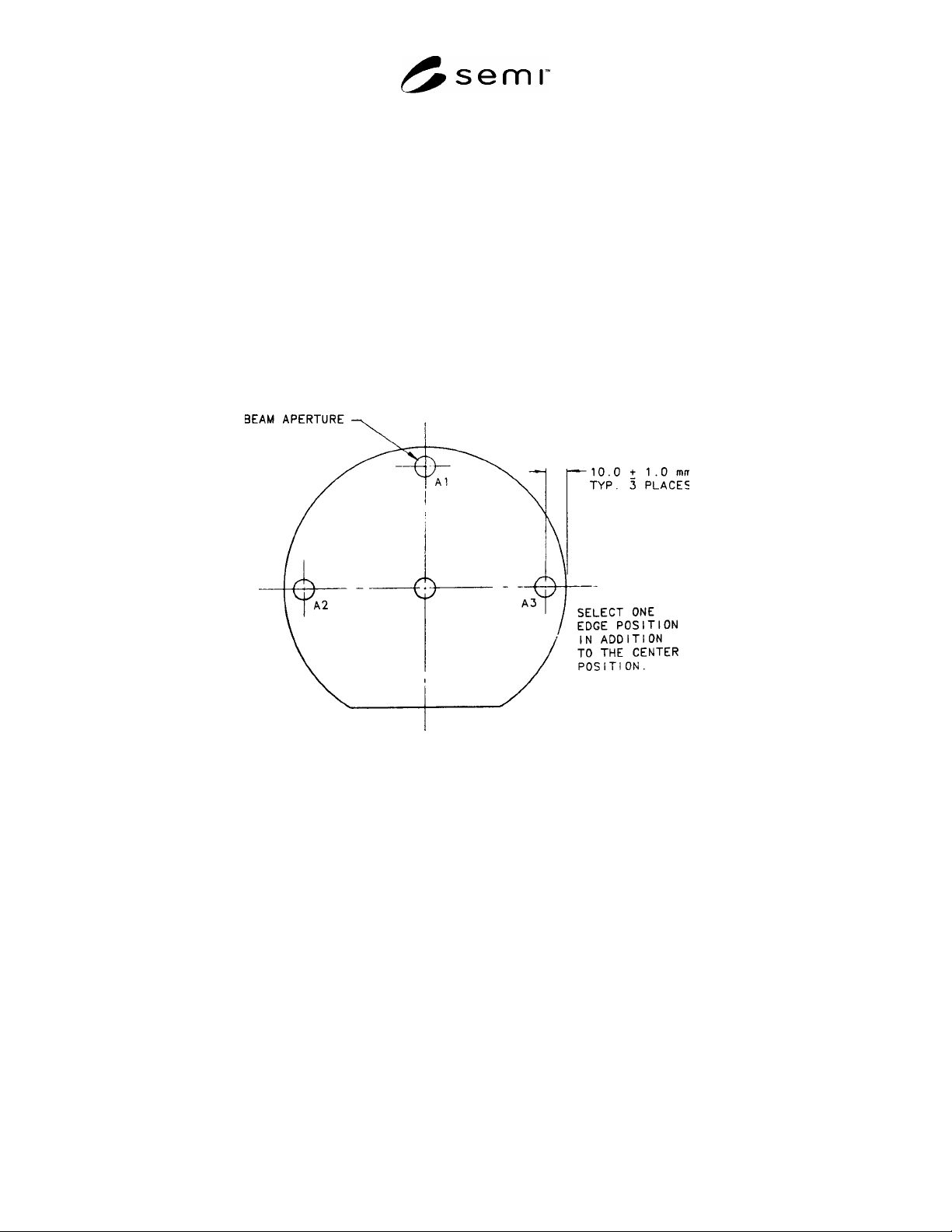
8.1.1 This test plan consists of measurements (1) at the center of the wafer, located within 3 mm of the intersection
of any two diameters that are at least 45 apart, and (2) at one position 10.0 ± 1 mm from the sample periphery on
one of the diameters parallel with or perpendicular to the major flat (or, for notched wafers, perpendicular to or
parallel with the notch axis).
8.1.2 The positions of edge measurement sites are determined by the distance from the sample periphery to the
center of the aperture.
8.1.3 The position A1 on the diameter perpendicular to the major flat (parallel with the notch axis) and at the side of
the wafer opposite the major flat (or notch) is preferred (see Figure 1). Positions A2 and A3 on the diameter parallel
with the major flat (perpendicular to the notch axis) may be selected to replace position A1 if agreed to by both
customer and supplier. Specify Test Plan A1, Test Plan A2, or Test Plan A3 depending on the position selected.
8.1.4 When an interfering minor flat is present, locate the edge position as though the minor flat were not present.
Figure 1
Test Plan A
8.2 Test Plan B
8.2.1 This test plan consists of measurements at the center of the wafer, located within 3 mm of the intersection of
any two diameters that are at least 45 apart, and at two positions 10.0 ± 1 mm from the sample periphery on each
end of the diameter parallel with the major flat (or, for notched wafers, perpendicular to the notch axis) (see Figure
2).
8.2.2 In addition, two optional measurements may be made at the half radius [(R/2) ± 1 mm] positions on the same
diameter of the wafer. If made, these optional measurements must be in addition to measurements at the center and
two edge positions. Customer and supplier must agree on the use of measurements at R/2 positions. Specify Test
Plan B1 when using all five positions.
8.2.3 When an interfering minor flat is present, locate the edge position as though the minor flat were not present.