semi合集-English.pdf - 第7211页
SEMI MF26-0305 © SEMI 2003, 2005 1 SEMI MF26-0305 TEST METHODS FOR DETERMINING THE ORIENTATION OF A SEMICONDUCTIVE SI NGLE CRYSTAL These test methods were techni cally approved by the Global Silicon W a fer Comm ittee an…

SEMI ME1392-0305 © SEMI 2003, 2005 19
D
ATA SEQUENCE
This section of the data file is a list of all data for the measurement. Each data point is stored
on a separate line ending in a carriage return—line feed pair. Separate variables in the line
are delimitated with commas. There is no imposed limit to the number of variables in the
line. Variables that do not change from the data point to the next do not have to be repeated,
but two commas are needed to reserve the column.
NOTICE: SEMI makes no warranties or representations as to the suitability of the standards set forth herein for any
particular application. The determination of the suitability of the standard is solely the responsibility of the user.
Users are cautioned to refer to manufacturer's instructions, product labels, product data sheets, and other relevant
literature, respecting any materials or equipment mentioned herein. These standards are subject to change without
notice.
By publication of this standard, Semiconductor Equipment and Materials International (SEMI) takes no position
respecting the validity of any patent rights or copyrights asserted in connection with any items mentioned in this
standard. Users of this standard are expressly advised that determination of any such patent rights or copyrights, and
the risk of infringement of such rights are entirely their own responsibility.
Copyright by SEMI® (Semiconductor Equipment and Materials
International), 3081 Zanker Road, San Jose, CA 95134. Reproduction of
the contents in whole or in part is forbidden without express written
consent of SEMI.

SEMI MF26-0305 © SEMI 2003, 2005 1
SEMI MF26-0305
TEST METHODS FOR DETERMINING THE ORIENTATION OF A
SEMICONDUCTIVE SINGLE CRYSTAL
These test methods were technically approved by the Global Silicon Wafer Committee and are the direct
responsibility of the North American Silicon Wafer Committee. Current edition approved for publication by
the North American Regional Standards Committee on December 10, 2004. Initially available at
www.semi.org February 2005; to be published March 2005. Original edition published by ASTM
International as ASTM E 26-63T. Last previous edition SEMI MF26-87a (Reapproved 1999).
1 Purpose
1.1 The orientation of semiconductor crystals and wafers as determined by these test methods is an important
materials acceptance requirement because the orientation controls various parameters of semiconductor devices
fabricated from the material.
2 Scope
2.1 These test methods cover techniques for determining the crystallographic orientation of a surface which is
roughly parallel to a low-index atomic plane in single crystals used primarily for semiconductor devices.
NOTE 1: DIN 50433 contains equivalent methods. It is the responsibility of DIN Committee NMP 221. DIN 50433, Testing of
Inorganic Semiconductor Materials: Determining the Orientation of Monocrystals; Part 1 with an X-ray Goniometer, and Part 2
by the Light-figure Method, is available from Beuth Verlag GmbH, Burggrafenstrasse 6, 10787 Berlin, Germany, Website:
www.beuth.de.
2.2 Two types of test methods are covered as follows:
2.2.1 Test Method A, X-ray Diffraction Orientation — This test method may be used for the orientation of all
semiconductive single crystals. The X-ray test method is nondestructive and yields the more precise measurement
of orientation; however, use of the equipment requires compliance with stringent safety regulations.
2.2.2 Test Method B, Optical Orientation — This test method is limited in application at the present time to
elemental semiconductors. The optical test method requires etching the specimen and is therefore destructive of
polished wafer surfaces. This test method is less precise than the X-ray test; however, the apparatus required is less
complex.
NOTICE: This standard does not purport to address safety issues, if any, associated with its use. It is the
responsibility of the user of this standard to establish appropriate safety and health guides and determine the
applicability of regulatory or other limitations prior to use.
3 Referenced Standards
3.1 SEMI Standards
SEMI C28 — Specifications and Guidelines for Hydrofluoric Acid
SEMI C30 — Specifications and Guidelines for Hydrogen Peroxide
SEMI C40 — Specification for Potassium Hydroxide, 45% Solution
SEMI C43 — Specification for Sodium Hydroxide, 50% Solution
3.2 ASTM Standards
D 5127 — Guide for Ultra Pure Water Used in the Electronics and Semiconductor Industry
1
E 82 — Test Method for Determining the Orientation of a Metal Crystal
2
1 Annual Book of ASTM Standards, Vol 11.01, ASTM International, 100 Barr Harbor Drive, West Conshohocken, PA 19428. Telephone: 610-
832-9500, Fax: 610-832-9555, Website:
www.astm.org
2 Annual Book of ASTM Standards, Vol 03.01.
SEMI MF26-0305 © SEMI 2003, 2005 2
E 177 — Practice for Use of the Terms Precision and Bias in ASTM Test Methods
3
3.3 ANSI Standard
B74.10 — Specifications for Grading of Abrasive Microgrits
4
3.4 Other Standard
Code of Federal Regulations, Title 10, Part 20, Standards for Protection Against Radiation
5
NOTICE: Unless otherwise indicated, all documents cited shall be the latest published versions.
4 Test Method A — X-Ray Diffraction Orientation
4.1 Summary of Test Method
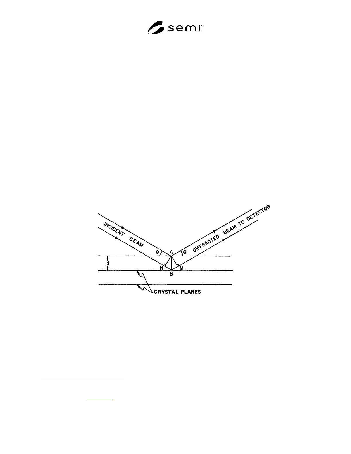
4.1.1 The atoms of a single crystal form a periodic three-dimensional array in a crystal lattice structure whose units
may be considered as lying in a series of parallel planes of equal perpendicular spacing, d, as shown in Figure 1.
When a beam of parallel, monochromatic X rays of wavelength
is incident upon the planes, diffraction (reflection)
occurs when the path difference of the X rays between adjacent planes is an integral number, n, of wavelengths.
When this geometrical condition is satisfied, the reflections from the various planes of the series are exactly in phase
and the diffracted beam is of maximum intensity. Thus, as shown in Figure 1, the diffracted beam of X rays
possesses maximum intensity when the angle of incidence,
, of the beam with the reflecting planes, the X-ray
wave-length,
, the atomic interplanar spacing, d, and the order of the diffraction, n, simultaneously have values that
obey Bragg’s law as follows:
sin2dn
(1)
NOTE: Reflection conditions are as follows: NB = BM = dsin
, NB + BM = n
, n
= 2dsin
.
Figure 1
Geometrical Reflection Conditions for X Rays from a Single Crystal
4.1.1.1 The reflecting planes are more commonly defined in terms of their Miller indexes (h, k, l). The Miller
indexes are the smallest integers proportional to the reciprocals of the intercepts of the plane on the three crystal
axes of unit length. Thus, for any lattice structure where the periodicity is represented by a cubic unit cell of side
length (lattice parameter), a, the lattice spacing, d, of a set of parallel atomic planes, may be written as follows:
3 Annual Book of ASTM Standards, Vol 14.02.
4 American National Standards Institute, New York Office: 25 West 43rd Street, New York, NY 10036, USA. Telephone: 212-642-4900; Fax:
212-398-0023, Website:
www.ansi.org
.
5 Published in Federal Register, Nov. 17, 1960. Available from Superintendent of Documents, U.S. Government Printing Office, Washington,
DC 20402.