semi合集-English.pdf - 第7261页
SEMI MF657-0705 © SEMI 2003, 2005 7 min max ) ( ) ( TTV a b a b (2) where: a = distance between the top s urface of the wafer under test and the upper probe, in. (or m), b = distance between the bottom surf ace…
SEMI MF657-0705 © SEMI 2003, 2005 6
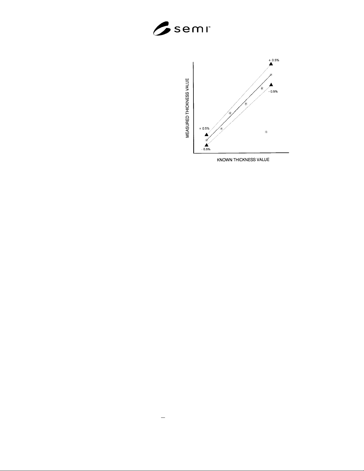
values. Observe the plotted points. If all points fall on or within the limit lines, accept the apparatus as satisfying
the linearity requirement for the test (see Figure 3).
9.2 Verify that the specified requirement is met for
parallelism of the plane defined by the reference ring
and the working surface of the surface plate.
9.2.1 Set up the equipment to accept the flat. Insert
the precision metal flat in the specimen position (if
one side of the flat is known to be flatter than the
other, insert the flat with that side facing the surface
plate).
9.2.2 Measure and record the distance between the
bottom probe and the bottom surface of the precision
flat as the flat is scanned in accordance with the
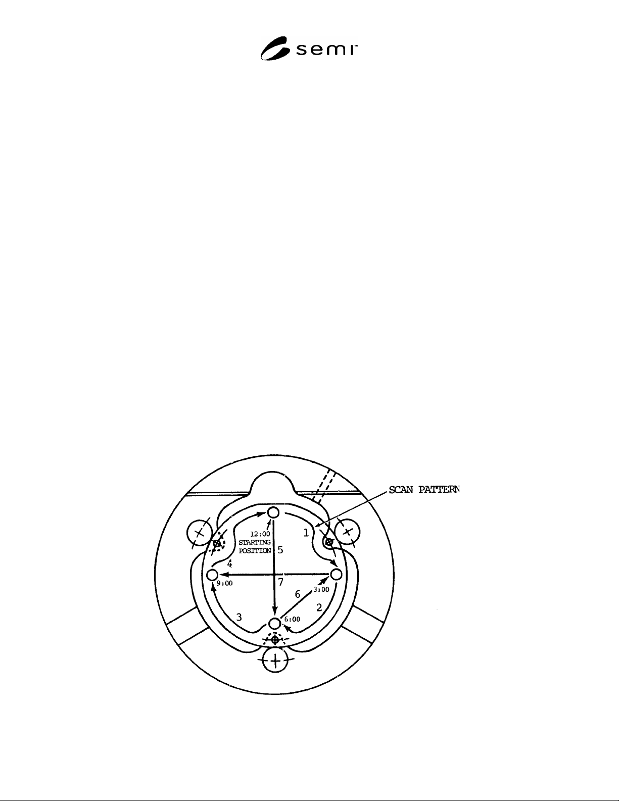
pattern shown in Figure 4. Remove the flat.
9.2.3 Inspect the recorded distance values and
calculate the difference between the maximum and
minimum value.
9.2.4 If the difference calculated in ¶9.2.3 is less than
or equal to 1.5 m (or 60 in.), accept the apparatus as satisfying the parallelism requirement.
NOTE 7: The value 1.5 m (or 60 in.) represents the total system transfer error of the reference ring together with the surface
plate and is intentionally greater than the tolerance of 1.0 m (or 40 in.) given for the parallelism of the defined plane of the
reference ring and the bottom surface of the ring.
10 Procedure
10.1 If not already assembled, assemble the apparatus with the selected reference ring corresponding to the intended
specimen size on the surface plate and the matching guide in position to limit ring movement. Make sure that the
probes are in the parking position and that the position is away from the operator (see Figure 2).
10.2 Place the test specimen on the support pads with the primary flat parallel with the flat orientation line and with
the periphery of the test specimen against the two guide pins closest to the probe parking position.
10.3 Move the ring on the surface plate until the probes are at the starting position of the scan.
10.4 Reset the indicator.
10.5 Move the reference ring on the surface plate to scan the probes along the curved and straight segments 1
through 7 (see Figure 4).
10.6 Record, in inches or micrometres, the individual displacements of the top and bottom surfaces at selected
points along the scan pattern or, for direct-reading instruments, the difference between the largest and smallest of the
differences or sums of the paired displacements, depending on whether warp (differences) or TTV (sums) is being
measured.
10.7 For referee measurements only, repeat ¶¶10.4 through 10.7 nine more times.
10.8 Position the ring so that the probes are in the parking position and remove the specimen.
10.9 Repeat ¶¶10.2 through 10.8 for each wafer to be measured.
11 Calculations
11.1 Unless the instrument is direct reading, calculate for each wafer the difference between each pair of
displacement values a and b and inspect the differences to identify the maximum and minimum difference values.
Calculate the warp or TTV in micrometers or inches according to the appropriate relation:
minmax
)()(
2
1
warp abab (1)
= Thickness of Master
Fi
g
ure 3
Thickness Gauge Linearity Check
SEMI MF657-0705 © SEMI 2003, 2005 7
minmax
)()(TTV abab
(2)
where:
a =
distance between the top surface of the wafer under test and the upper probe, in. (or m),
b =
distance between the bottom surface of the wafer under test and the lower probe, in. (or m),
max denotes the largest value of the difference or sum, and
min denotes the smallest value of the difference or sum.
11.2 For routine measurements, record the calculated value(s) of warp or TTV or both.
11.3 For referee measurements:
11.3.1 Calculate each measured warp or TTV from Equation 1 or Equation 2, respectively.
11.3.2 Then calculate the mean value and standard deviation.
11.3.3 Record the mean value as the warp or TTV, as appropriate.
12 Report
12.1 Report the following information:
12.1.1 Date of test,
12.1.2 Location of test,
12.1.3 Identification of operator,
12.1.4 Identification of measuring instrument(s),
12.1.5 Lot identification, including nominal diameter and thickness,
12.1.6 Description of sampling plan, and
12.1.7 Warp or TTV (or both) of each wafer measured, m or (in.)
Figure 4
Measurement Scan Pattern
SEMI MF657-0705 © SEMI 2003, 2005 8
12.2 For referee tests the report shall also include the standard deviation of the warp or TTV (or both) of each wafer
measured, m or (in.).
13 Precision and Bias
13.1 A round-robin experiment was conducted to estimate the precision of this test method.
3
Each of 11
laboratories was to perform three measurements on five 100 mm and five 125 mm diameter polished wafers. The
wafers in each set of five had warp values from about 6 to about 40 m, and TTV values from about 1 to about 5
m.
13.2 Three laboratories used warp measuring equipment that did not conform to the requirements of this test
method, and one additional laboratory did not supply warp data. Two laboratories used TTV measuring equipment
that did not conform to the requirements of this test method. Data from these laboratories were excluded from the
analysis.
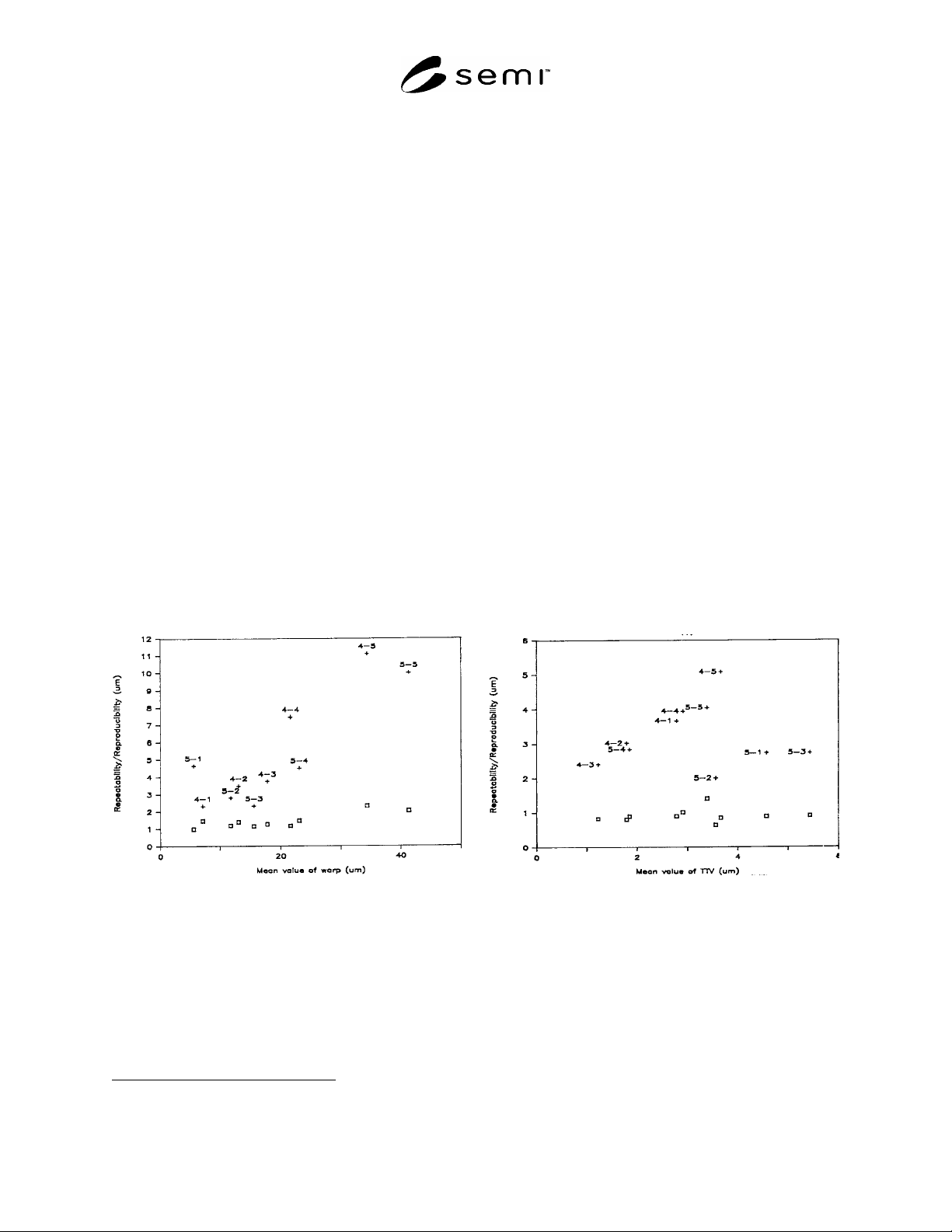
13.3 Based on warp results from seven laboratories and TTV results from nine laboratories, the repeatability (within
laboratory) is estimated to be 1.45 ± 0.42 m and 0.92 ± 0.20 m for warp and TTV, respectively. No significant
difference was noted between measurements on 100 and on 125 mm diameter wafers. There was no significant
trend in repeatability with measured value (see Figure 5).
13.4 The reproducibility (between laboratories) is estimated to be 5.25 ± 3.19 m and 3.25 ± 0.92 m for warp and
TTV, respectively. In this case, there was some increase in the value of warp reproducibility as the warp value
increased and a less pronounced increase in the value of TTV reproducibility as the TTV value increased (see Figure
6).
NOTE 8: In these figures, the numbers are identification numbers. The initial digit represents the approximate nominal diameter
of the sample wafers in inches
13.5 No statement of bias can be made because there are no reference standards against which the result of this
measurement can be compared.
Repeatabilit
y
+
Reproducibility
Repeatabilit
y
+
Reproducibility
Figure 5 Figure 6
Repeatability and Reproducibility of Warp Values Repeatability and Reproducibility of TTV Values
Determined by Interlaboratory Experiment Determined by Interlaboratory Experiment
14 Keywords
14.1 measurement of warp and total thickness variation, (TTV); noncontact scanning; silicon wafers; thickness
variation; warp
3 Supporting data are available on request from SEMI Headquarters, 3081 Zanker Road, San Jose, CA, Telephone 408-943-7021, Fax: 408-943-
7015, e-mail: standards@semi.org. Request International Standards Research Report 1005.