semi合集-English.pdf - 第6513页
SEMI G80-0200 © SE MI 2000 21 Table A1-1 (co nt.) Test Method S ummar y - Non Data Analy s is Aspects Associate d with This Method D r i v e to C o m p a r e E r ror = R e f e r e n c e - [ ( M i n V a lu e + M a x V a l…
SEMI G80-0200 © SEMI 2000 20
APPENDIX 1
NOTE: The material in this appendix is an official part of SEMI G80 and was approved by fulll letter ballot procedures on
September 3, 1999 by the North Amerian Regional Standards Committee.
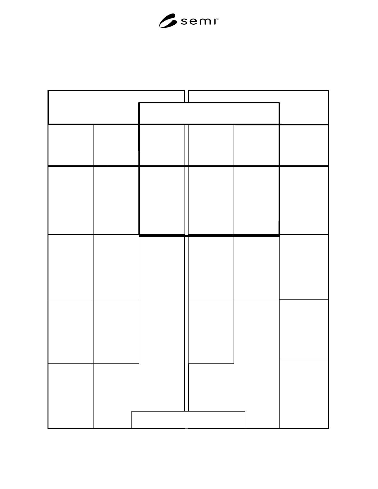
Table A1-1 Test Method Summary Table for Establishing Overall Timing Accuracy (OTA)
LEVEL 1
Timing Linearity
Extended Delay
Multiple Period
Data below represents
Level 1 edge-delay
results
LEVEL 2
High Speed Clock
Accuracy
_
_________________
_
Drive Input Z
Timing Error
Level 1 (Section
10.3.5) Z to 0
(Low)
_
_____________
_
_____________
Timing Linearity
Level 1
(Sec.10.3.1)
Positive Error:
_________________
Negative Error:
_________________
b) High Speed
Clock Transition
Time Variation
Level 2 (Section
10.4.3- Drive Input
Transition Time
for clock function)
_
______________
a) High Speed
Clock Delay Error
Level 2 (Section
10.4.1- Drive Input
Timing Delay for
clock function)
_
______________
Extended Delay
Level 1 (Sec.
10.3.4)
Positive Error:
_________________
Negative Error:
_
_______________
Multiple Period
Level 1 Optional
(Sec. 10.3.6)
Positive Error:
_________________
Negative Error:
_
________________
Drive Input Z
Timing Error
Level 1 (Section
10.3.5) Z to 1
(High)
_
_____________
_
_____________
Drive Input Z
Timing Error
Level 1 (Section
10.3.5) 0 (Low)
to Z
_
_____________
_
_____________
Drive Input Z
Timing Error
Level 1 (Section
10.3.5) 1 (High)
to Z
_
_____________
_
_____________
1) Drive Input
To Compare
Output Timing
_
_______________
_
3) Compare
Output Edge
Placement
_
_______________
2) Drive
Input Edge
Placement
_
_______________
_
Drive Input to
Compare Out put
Timing Accuracy
calculated from
the 10.3.1 entry.
_
_____________
a) Compare
Output Time
Delay Error
Level 2 (Section
10.4.2)
_
_____________
a) Drive Input
Timing Delay
Error Level 2
(Section 10.4.1)
_
_____________
b) Drive Input
Transition Time
Variation
Level 2 (Section
10.4.3)
_
_____________
c) Drive Input
Timing Cycle
Jitter Level 2
(Section 10.4.4)
_
____________
Single Point Overall Timing Accuracy (OTA) Results
D
ata to enter here is: A = Dr (item 2) + Cmp (item 3) + Dr-Cmp (item 1)
-B = -Dr (item 2) - Cmp (item 3) + Dr-Cmp (item 1)
.
Drive Z Timing
Data below
represents Level 1 Z-
state timing results
c) High Speed
Clock Cycle Jitter
Level 2 (Section
10.4.5)
_
______________
d) High Speed
Clock Phase Jitter
Level 2 (Section
10.4.6)
_
______________
The user of the method is advised to read Section
13, Precautions before filling in this table.
SEMI G80-0200 © SEMI 200021
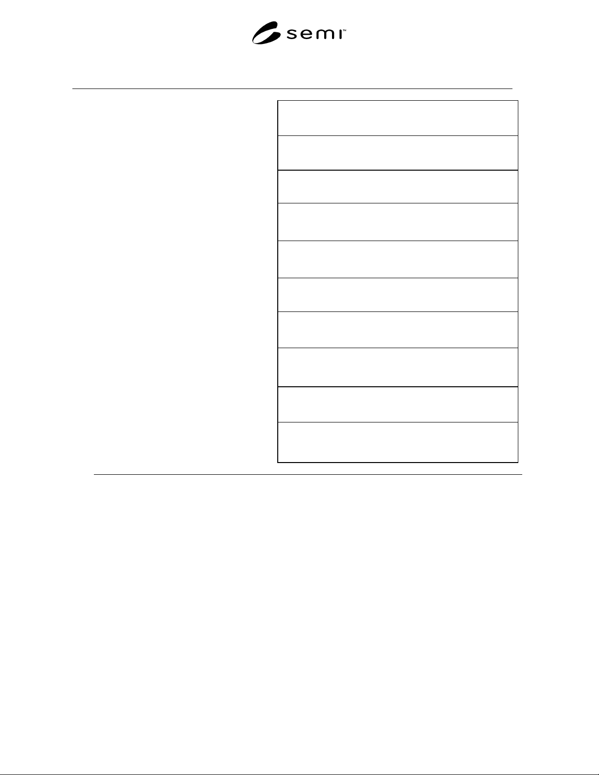
Table A1-1 (cont.) Test Method Summary - Non Data Analysis Aspects Associated with This Method
Drive to Compare Error = Reference - [(Min Value + Max Value)/2]
1. Level 1 –– Procedure Start Date and Time:
4. Level 2 –– Procedure Finish Data and Time:
5. Specify the ambient temperature when this
method was executed.
6. Manufacturer's model number and/or name for
this system analyzed.
7. System Serial Number:
8. Date and Time of Last System Calibration:
9. Specify PARTIAL or Full-Up execution of
this method. Exceptions noted in Appendix 3.
3. Level 2 –– Procedure Start Date and Time:
2. Level 1 –– Procedure Finish Date and Time:
10. Specify number of Test Heads and number of
Pins analyzed using this method.

SEMI G80-0200 © SEMI 2000 22
APPENDIX 2
NOTE: The material in this appendix is an official part of SEMI G80 and was approved by fulll letter ballot procedures on
September 3, 1999 by the North Amerian Regional Standards Committee.
A2-1 Examples
NOTE 1: This appendix contains Figures A2-1, A2-2, A2-3,
and A2-4 created for this method as examples. The purpose of
these examples is to show that Drive Input To Compare
Output Error (Accuracy) can be determined. Establishing this
value requires that two edge timing values be detected: MIN
DRIVE VALUE: the earliest occurrence the drive edges with
the latest compare edge. That is also referred to here as
FIRST PASS. MAX DRIVE VALUE: the latest occurrence
of the drive edges with the earliest compare edge. That is also
referred to here as LAST FAIL.
NOTE 2: Timing Linearity Test 10.3.1 can provide these
values. Examples in this appendix will also show data entry
to Table 2 for OTA calculation.
A2-1.1 Maximum Drive Value and Minimum Drive
Value — To follow this analysis you can refer to the
example in Figure 7. In this example drive error and
compare error are each 100ps.
NOTE 3: Figures A2-1, A2-2, A2-3, and A2-4 are equivalent
and represent complementary examples for the cases where
drive error does not have the same error value as compare
error.
A2-1.2 Minimum Drive Value is determined by first
assuming that all compare edges are programmed at
0ns. You must then take into account the drive to
compare error, in this example that value is –50ps (note
the sign indicating the shift is in the negative direction).
Add the drive to compare error to the compare
programming value. That means that the average
(mean) compare edge can be thought of as actually
occurring at –50ps (versus the programmed value of
0ns ). Per this example the compare error is ± 100ps,
which means the latest compare edge would occur at +
50ps (–50ps + 100ps). Since the driver edge error is
also ± 100ps and is programmed to the reference value
of 1000ps, the earliest drive edge occurs at 900ps
(1000ps minus 100ps). The MIN DRIVE VALUE is
then whatever programming value is needed to get the
latest compare edge (at + 50ps) to line up with the
earliest drive edge (at 900ps). In this case that's 850ps
(the difference between 50ps and 900ps). This value of
850ps is also referred to at the FIRST PASS.
A2-1.3 The same analysis applies when determining
Max Drive Value. First assume all compare edges are
programmed to 0ns. The drive to compare error must
be added-in, in this case –50ps. That puts the mean
programmed compare edge at –50ps. Taking into
account the compare edge error of 100ps the earliest
compare edge would occur at –150ps. The drive edges
are programmed to 1000ps. Thus the latest drive edge
occurs at 1100ps when the 100ps drive edge error is
taken onto account. To get the earliest compare edge to
line up with the latest drive edge 1250ps of delay would
need to be programmed (the difference between 1100ps
and –150ps). This value of 1250ps is referred to as the
LAST FAIL.
A2-1.4 Drive to Compare Edge Error — By definition
DRIVE TO COMPARE EDGE ERROR is the relative
time difference between the drive (input) edge error and
compare (output) edge error distributions. All drive
edges in Level 1 are detected in parallel in pairs. Once
the minimum and maximum values of drive edge are
determined per procedure 10.3.1 (illustrated in Figures
A2-1 through A2-4) determination of drive to compare
edge error can be established. As per these examples
(Figures 7 and A2-1 through A2-4) the drive to
compare edge error is calculated as the reference value
minus the average of min and max error values:
Drive to Compare Error =
Reference-[Min Value + Max Value)/2]
A2-1.5 Distinguishing Drive and Compare Edge Error
Uniquely Is Not Possible with Level 1 Tests — The user
is cautioned that even though drive to compare edge
error is known, per this method it is still not possible to
distinguish Level 1 drive input error from compare
output error. The key to this shortcoming lies in
observation of examples shown in Figures A2-1
thorough A2-4. These examples have drive and
compare edge error values that are not the same value.
That is, drive error is either much greater that compare
edge error, or vice versa. In each example drive to
compare edge error is established. To establish the
point that drive input error cannot be distinguished from
compare output error per level 1, the user is asked to
look at Figures A2-1 and A2-2. In these two examples
it is assumed that the drive error and compare error are
different by a factor of two. Because of limited
visibility per the level 1 approach it is not possible to
determine that the drive error is ± 100ps and the
compare error is ± 50ps (example in Figure A2-1), or
vice versa. All that can be established is that the
positive error is 200ps and the negative error is 100ps.
Level 2 tests are required to determine drive input
timing error and compare output timing error.
A2-1.6 The same rationale applies for the examples in
Figure A2-3 and A2-4 where one component of error is
assumed to be 200ps and the other is 100ps, with a 50ps
drive to compare error. The drive to compare edge
error is determined, but again establishing a unique
value for drive or a unique value compare error is not