semi合集-English.pdf - 第5071页
SEMI M22-0303 © SEMI 1992, 2003 6 NOTICE: SEMI makes no warranties or representations as to the su itability of the standard set forth herein for any particular application . The determinati on of the suitability o f the…
SEMI M22-0303 © SEMI 1992, 2003 5
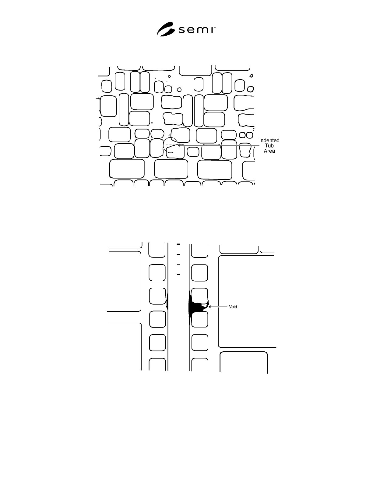
Figure 3
Pattern Deformation
Figure 4
Void in the Polycrystalline Silicon

SEMI M22-0303 © SEMI 1992, 2003 6
NOTICE: SEMI makes no warranties or representations as to the suitability of the standard set forth herein for any
particular application. The determination of the suitability of the standard is solely the responsibility of the user.
Users are cautioned to refer to manufacturer’s instructions, product labels, product data sheets, and other relevant
literature respecting any materials or equipment mentioned herein. These standards are subject to change without
notice.
By publication of this standard, SEMI takes no position respecting the validity of any patent rights or copyrights
asserted in connection with any item mentioned in this standard. Users of this standard are expressly advised that
determination of any such patent rights or copyrights, and the risk of infringement of such rights, are entirely their
own responsibility.
Copyright by SEMI® (Semiconductor Equipment and Materials
International), 3081 Zanker Road, San Jose, CA 95134. Reproduction o
f
the contents in whole or in part is forbidden without express written
consent of SEMI.
SEMI M23-0703 © SEMI 1993, 2003 1
SEMI M23-0703
SPECIFICATION FOR POLISHED MONOCRYSTALLINE INDIUM
PHOSPHIDE WAFERS
This specification was technically approved by the Global Compound Semiconductor Committee and is the
direct responsibility of the North American Compound Semiconductor Committee. Current edition approved
by the North American Regional Standards Committee on November 27, 2001. Initially available at
www.semi.org December 2001; to be published March 2002. Originally published in 1993; previously
published October 2000.
NOTICE: The designation of SEMI M23 was updated
during the 0703 publishing cycle to reflect the addition
of SEMI M23.6.
1 Purpose
1.1 These specifications cover the substrate require-
ments for monocrystalline high-purity indium phos-
phide wafers used in semiconductor and electronic
device manufacturing. Dimensional and crystallo-
graphic orientation characteristics are the only standard-
ized properties set forth below.
1.2 A complete purchase specification may require that
additional physical, electrical, and bulk properties be
defined. These properties are listed together with test
methods suitable for determining their magnitude where
such procedures are documented.
2 Scope
2.1 These specifications are directed specifically to
indium phosphide wafers with one or both sides
polished. Unpolished wafers or wafers with epitaxial
films are not covered; however, purchasers of such
wafers may find these specifications helpful in defining
their requirements.
2.2 The material is Single Crystal Indium Phosphide
(InP) having a cubic zinc blende structure and the
following properties:
Density 4.787 g/cm
3
Melting Point
1062°C
Dielectric Constant 12.4
Lattice Parameter
5.869 Α at 27° C
Energy Gap 1.351 eV at 27° C
2.3 For reference purposes SI (System International,
commonly called metric) units shall be used.
2.4 This standard does not purport to address safety
issues, if any, associated with its use. It is the
responsibility of the users of this standard to establish
appropriate safety and health practices and determine
the applicability of regulatory limitations prior to use.
3 Referenced Standards
3.1 SEMI Standards
SEMI M39 — Test Method for Measuring Resistivity
and Hall Coefficient and Determining Hall Mobility on
Semi-Insulating GaAs Single Crystals
3.2 ASTM Standards
1
ASTM E122 — Practice for Choice of Sample Size to
Estimate Average Quality of a Lot or Process
ASTM F26 — Test Methods for Determining the
Orientation of a Semiconductive Single Crystal
ASTM F42 — Test Method for Conductivity Type of
Extrinsic Semiconducting Materials
ASTM F76 — Test Methods for Measuring Resistivity
and Hall Coefficient and Determining Hall Mobility in
Single Crystal Semiconductors
ASTM F84 — Test Methods for Measuring Resistivity
of Silicon Wafers with an In-Line Four-Point Probe
ASTM F154 — Practices and Nomenclature for
Identification of Structures and Contaminants Seen on
Specular Silicon Surfaces
ASTM F523 — Practice for Unaided Visual Inspection
of Polished Silicon Wafer Surfaces
ASTM F533 — Test Method for Thickness and
Thickness Variation of Silicon Wafers
ASTM F534 — Test Method for Bow of Silicon
Wafers
ASTM F613 — Test Method for Measuring Diameter
of Semiconductor Wafers
ASTM F657 — Test Method for Measuring Warp and
Total Thickness Variation on Silicon Wafers by Non-
Contact Scanning
ASTM F671 — Test Method for Measuring Flat Length
on Wafers of Silicon and Other Electronic Materials
1 American Society for Testing and Materials, 100 Barr Harbor
Drive, West Conshohocken, PA 19428-2959 (All cited standards
except for E122 may be found in Volume 10.05 of the Annual Book
of ASTM Standards; E122 may be found in Volume 14.02.)