semi合集-English.pdf - 第161页
SEMI E21-94 © SEMI 1991, 2002 1 SEMI E21-94 (Reapproved 1102) CLUSTER TOOL MODULE INTERF ACE: MECHANICAL INTERFACE AND WAFER TRANSPORT STANDARD This standard was technically rea pproved by the Global Physical Interfaces …
SEMI E20-0697 © SEMI 1991, 2002 5
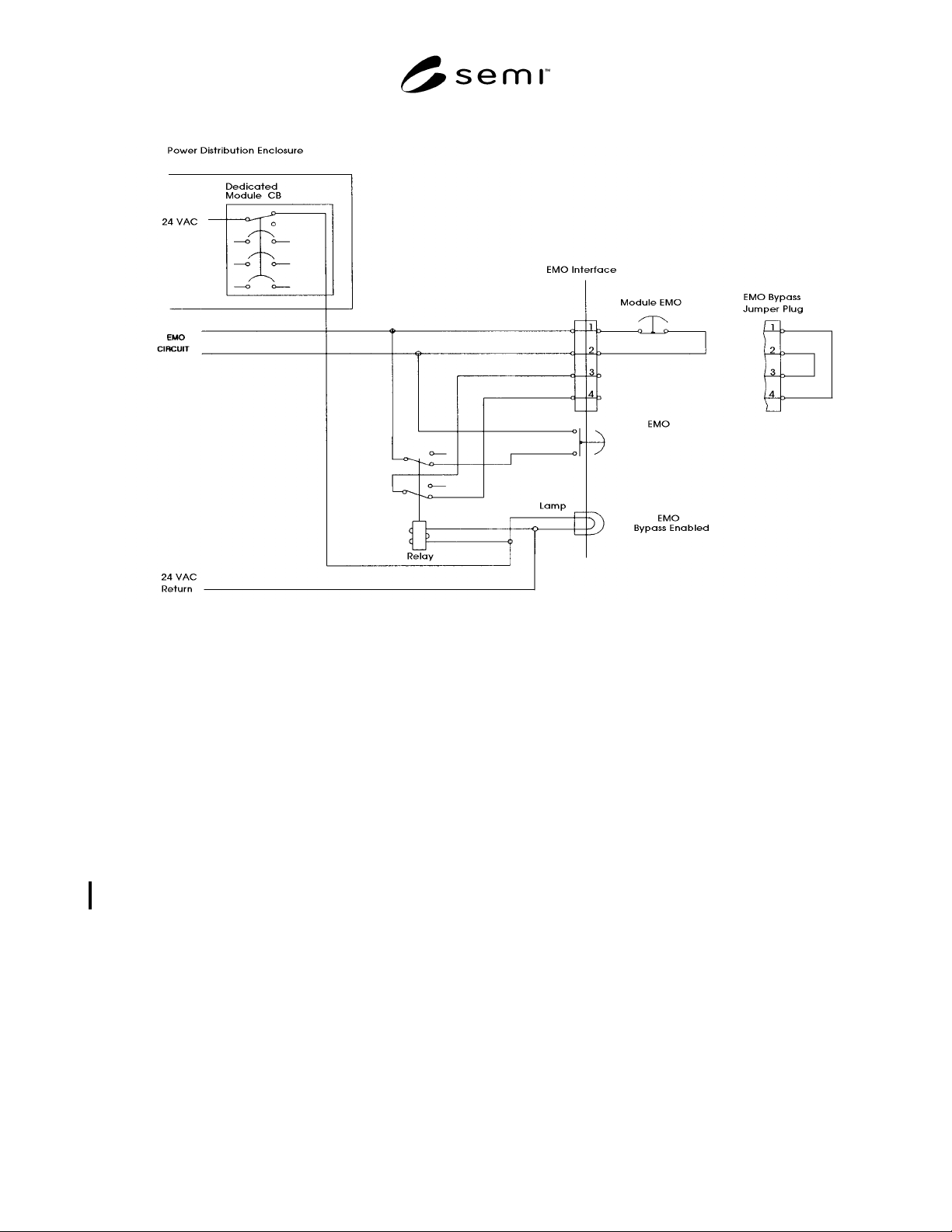
Figure R1-2
Example: EMO Connect/Disconnect Circuit(Module Power is “off,” as drawn.)
NOTICE: The user’s attention is called to the possibility that compliance with this standard may require use of an
invention covered by patent rights. By publication of this standard, Semiconductor Equipment and Materials
International (SEMI) takes no position respecting the validity of any patent rights asserted in connection with any
item mentioned in this standard. In particular, users of the specification should be aware that Drytek, Inc., A Unit of
General Signal, 16 Jonspin Road, Wilmington, MA 01887-1087, Phone: (508) 657-3933, has neither claimed nor
disclaimed that compliance with this specification would require use of an invention covered by one or more of its
patents. Users of this standard are expressly advised that determination of any such patent rights, and the risk of the
infringement of such rights, are entirely their own responsibility.
NOTICE: SEMI makes no warranties or representations as to the suitability of the standards set forth herein for any
particular application. The determination of the suitability of the standard is solely the responsibility of the user.
Users are cautioned to refer to manufacturer' s instructions, product labels, product data sheets, and other relevant
literature, respecting any materials or equipment mentioned herein. These standards are subject to change without
notice.
By publication of this standard, Semiconductor Equipment and Materials International (SEMI) takes no position
respecting the validity of any patent rights or copyrights asserted in connection with any items mentioned in this
standard. Users of this standard are expressly advised that determination of any such patent rights or copyrights, and
the risk of infringement of such rights are entirely their own responsibility.
Copyright by SEMI® (Semiconductor Equipment and Materials
International), 3081 Zanker Road, San Jose, CA 95134. Reproduction o
f
the contents in whole or in part is forbidden without express written
consent of SEMI.

SEMI E21-94 © SEMI 1991, 2002 1
SEMI E21-94 (Reapproved 1102)
CLUSTER TOOL MODULE INTERFACE: MECHANICAL INTERFACE
AND WAFER TRANSPORT STANDARD
This standard was technically reapproved by the Global Physical Interfaces & Carriers Committee and is the
direct responsibility of the North American Physical Interfaces & Carriers Committee. Current edition
reapproved by the North American Regional Standards Committee on July 21, 2002. Initially available at
www.semi.org October 2002; to be published November 2002. Originally published in 1991; previously
published in June 1999.
1 Purpose
1.1 The purpose of the standard is to simplify cluster
tool implementation in the fab. Equipment suppliers are
required to provide modules that can be connected into
any cluster tool using the specifications contained
herein.
1.1.1 Process and cassette modules accept wafers at
locations that may vary substantially from one module
to another. This places a burden on the capabilities of
transport modules to move wafers to and from various
modules in a cluster tool. This specification defines
wafer transport planes within cassette and process
modules. This obviates the wafer transport problem to a
large extent, but does not unduly restrict module
content.
2 Scope
2.1 The standard defines the interface plane between
modules in a cluster tool. It provides the mechanical
specifications at the interface that allow modules from
different suppliers to be connected together; no
requirements are imposed on the module content.
2.1.1 The standard is limited to wafers which are 200
mm (~ 8 in.) in diameter or smaller and to the interface
between cluster tool modules, with the following
exception. The transport module operates across the
interface plane; thus, a definition of the wafer transport
plane within cassette and process modules is required.
2.2 This standard does not purport to address safety
issues, if any, associated with its use. It is the
responsibility of the users of this standard to establish
appropriate safety health practices and determine the
applicability or regulatory limitations prior to use.
3 Impact
3.1 The adoption of the standard requires cluster tool
equipment designers to limit the wafer transport height
to a nominal value at the interface plane between two
modules. It also requires equipment designers to assure
that wafer transport planes within cassette and process
modules be clear for wafer transport. The transport
module requires the capability for a minimum reach
outside the module across the interface plane. Modules
may be connected using a quick connect/disconnect
clamping system. Constraints are placed on sealing
surfaces.
4 Referenced Standards
ISO 1609-1986 (E)
1
— “Vacuum Technology — Flange
Dimensions,” International Organization for
Standardization (ISO).
5 Terminology
5.1 Definitions
5.1.1 cassette module — a two-port module. One port
accepts or presents a cassette of wafers or possibly, in
an automated factory, an individual wafer for intertool
transport; the second port accepts or presents a single
wafer within the module for intratool transport.
5.1.2 cluster tool — an integrated, environmentally
isolated manufacturing system consisting of process,
transport, and cassette modules mechanically linked
together. The modules may or may not come from the
same supplier.
5.1.3 environmental isolation — separated from the
ambient atmospheric environment.
5.1.4 interface plane — the vertical surface defined by
the mating surfaces of two joined modules.
5.1.5 interface seal zone — an absolute surface or face
reserved for establishing an environmental seal between
modules.
5.1.6 intertool transport — wafer or cassette
movement between independent tools.
5.1.7 intratool transport — wafer movement inside a
cluster tool.
5.1.8 module — an independently-operable unit that is
part of a tool or system.
1 International Organization for Standardization, ISO Central
Secretariat, 1, rue de Varembé, Case postale 56, CH-1211 Geneva 20,
Switzerland. Telephone: 41.22.749.01.11; Fax: 41.22.733.34.30
Website: www.iso.ch

SEMI E21-94 © SEMI 1991, 2002 2
5.1.9 process module — a module that accepts or
presents a single wafer inside the module for intratool
transport.
5.1.10 reach — the distance measured from the
interface plane to the wafer centroid within a process or
cassette module.
5.1.11 transport module — a module that accepts or
presents a single wafer outside the module across the
interface plane for intratool transport.
5.1.12 wafer transport plane — the horizontal surface
a wafer traverses between modules.
5.1.13 wafer transport zone — the area of the interface
plane free of physical obstructions, reserved for wafer
movement between modules.
6 Requirements
6.1 Wafer Transport and Placement
6.1.1 Horizontal Transport Plane — The dimensions
for wafer placement during wafer transport are
referenced from the interface plane in the plan view
shown in Figure 1. The transport module is required to
present or accept a horizontal wafer outside the module
anywhere along an axis perpendicular to the center of
the interface plane to a maximum 305 mm (12 in.) from
the interface plane. Thus, a transport module is required
to have the capability to reach 305 mm (12 in.) beyond
its interface plane to a wafer centroid (see Section R1-
1). However, location of the wafer at a distance less
than 305 mm (12 in.) from the interface plane requires
that the transport module be capable of addressing the
intermediate location. Similarly, a cassette module or
process module accepts a horizontal wafer inside the
module anywhere along an axis perpendicular to the
center of its interface plane up to a maximum 305 mm
(12 in.) from the interface plane as required by the
application.
6.1.1.1 Placement Accuracy — The requirements for
placement accuracy of a wafer in the horizontal plane
within a module are 1.0 mm (0.04 in.) true position, ±
0.5 mm (± 0.020 in.) radially, with less than one degree
angular rotation for every module-to-transport-to-
module wafer transport (B
n
:A:B
n
+ 1as shown in Figure
1). If the wafer is displaced in the process module, it
must be returned to the original position within the non-
culmulative placement accuracy of 1.0 mm (0.04 in.)
true position, ± 0.5 mm (± 0.020 in.) radially.
6.1.2 Vertical Position of Transport Plane — The
elevation of the wafer transport plane is measured from
the facility floor as shown in Figure 2. The transport
module is required to present or accept a horizontal
wafer outside the module at a nominal wafer transport
height of 1100 mm (43.307 in.) from the facility floor
(see Section R1-2).
6.1.2.1 Vertical Motion — The transport module is
required to move the wafer to within ± 0.5 mm (0.020
in.) in the wafer transport plane. The transport module
is also required to posess a vertical motion capability to
a second plane 6.0 mm ± 0.5 mm (0.236 in. ± 0.020 in.)
below the wafer transport plane in order to allow wafer
handoff to or from passive cassette or process modules
(see Figure 2 and Section R1-3).
6.1.2.2 Reference Plane — The interface plane
alignment pins define a reference plane 9.5 mm (0.374
in.) below the wafer transport plane (see Figure 2).
6.2 Interface Plane — The interface plane contains the
interface seal zone and the wafer transport zone, which
do not overlap, and the location of the interface plane
alignment pins (see Figures 3 and 4).
6.2.1 Interface Seal Zone — The interface seal zone is
rectangular and symmetrically referenced to the
interface plane alignment pins. The inside boundary
dimension of the interface seal zone is 46 mm (1.811
in.) by 236 mm (9.291 in.). The outside boundary is 76
mm (2.992 in.) by 266 mm (10.472 in.). A seal zone is
either a seal surface or an O-ring face. All interface seal
zones facing toward a transport module are seal
surfaces polished to a surface finish less than or equal to
0.8 micrometer (32 microinches) parallel to the
circumference (see Section R1-4). All interface seal
zones facing toward a cassette or process module are O-
ring faces equipped with the appropriate capture groove
for the sealing method employed (see Figure 3 and
Section R1-4.1).
6.2.2 Wafer Transport Zone — The wafer transport
zone is the area within the interface seal zone reserved
for moving the wafer between modules. The wafer
transport zone which cannot be compromised by any
module is defined as the area at least 16 mm (0.630 in.)
above and below the alignment pin centerlines, and 111
mm (4.370 in.) to the left and right of the centerline
between the two alignment pins (see Figure 3 and
Section R1-5).
6.2.3 Interface Plane Alignment Pins — Provisions are
made for two 10 mm (0.394 in.) diameter locating pins
(see Figure 4) to be used as alignment aids between
modules. Under no circumstances should the flanges at
the interface plane and the alignment pins be subject to
a total load exceeding 500N (112 lbf) in shear. The
alignment pins have an absolute centerline separation of
300.0 mm (11.811 in.) in the horizontal plane. The pins
reside in the seal surface side of the flange pair,
opposite the O-ring, facing toward the transport
module. Mild press fit holes are provided in the seal
surface flange face. A clearance hole and a slot are