semi合集-English.pdf - 第2038页
SEMI E54.8-0305 © SEMI 1999, 2005 20 9.6.3.3 Table 35 shows the mappi ng of the SDM . 9.6.3.4 Objects specified in SEMI E54.11 are listed under the heading NCS Modu le reference. Every instance is allocated to a slot num…
SEMI E54.8-0305 © SEMI 1999, 2005 19
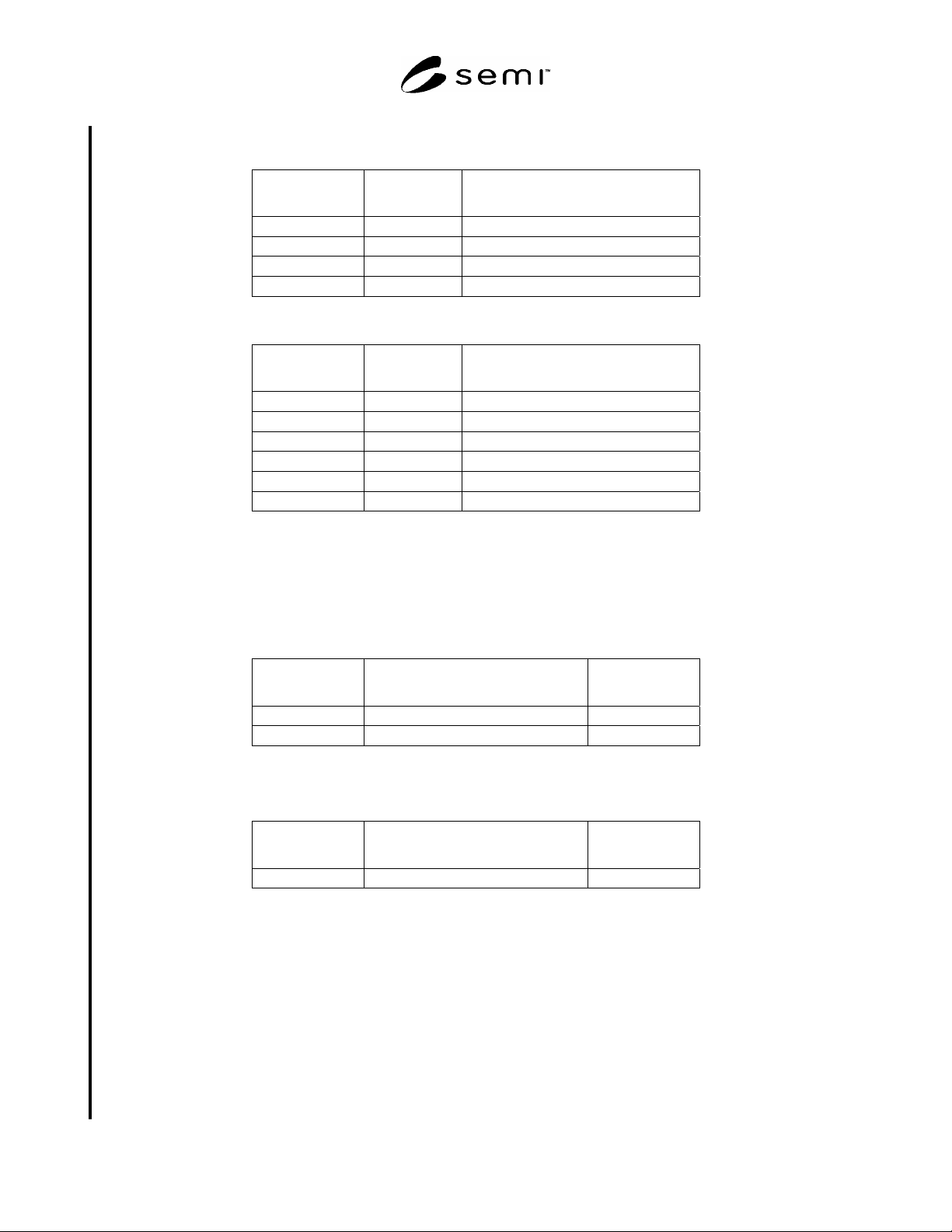
Table 31 Sensor AI-MNS Object Attribute Identifiers
SEMI SDM
Attribute ID
PROFIBUS
Index
Attribute
MnsA1 160 Reading Valid
MnsA2 161 Full Scale
MnsA3 162 Alarm Settling Time
MnsA4 163 Warning Settling Time
Table 32 Sensor AI-Counter Object Attribute Identifiers
SEMI SDM
Attribute ID
PROFIBUS
Index
Attribute
CounterA1 160 Reading Valid
CounterA2 161 Full Scale
CounterA3 162 Alarm Settling Time
CounterA4 163 Warning Settling Time
CounterA5 164 Upper Size
CounterA6 165 Lower Size
9.5.4 Services
9.5.4.1 The mapping of Service Tags and Identifiers is defined in §7 for SAC. The same method applies here for
the SDM.
9.5.4.2 The additional Services of DM are mapped as described in Table 33.
Table 33 DM additional Service Mapping
SEMI SDM Service
ID
Service Write Value to
Index 96
DmS1 Laser On 11
DmS2 Laser Off 12
9.5.4.3 The additional Services of SAC are mapped as described in Table 34.
Table 34 SAC Additional Service Mapping
SEMI SDM Service
ID
Service Write Value to
Index 64
SacS1 Clear Counts 11
9.6 Endpoint Device
9.6.1 Reference SEMI E54.11 for a complete specification of the SDM for Endpoint Devices.
9.6.2 Date-and-Time data structure shall be mapped to PROFIBUS data type Time Of Day. An Offset of 4383 has
to be added to Time Of Day day value to obtain the number of days since 1/1/72 (Time Of Day base is 1/1/84).
9.6.3 Objects
9.6.3.1 Consistent with SEMI E54.11 and ¶7.4 above, the DM and SAC objects are identified as Object 1 and
Object 2, respectively.
9.6.3.2 Notice that references for the Local Link Objects are not included; the existence of these objects are implied
by behavior and not explicitly included. Therefore, these objects are not accessible from the network.
SEMI E54.8-0305 © SEMI 1999, 2005 20
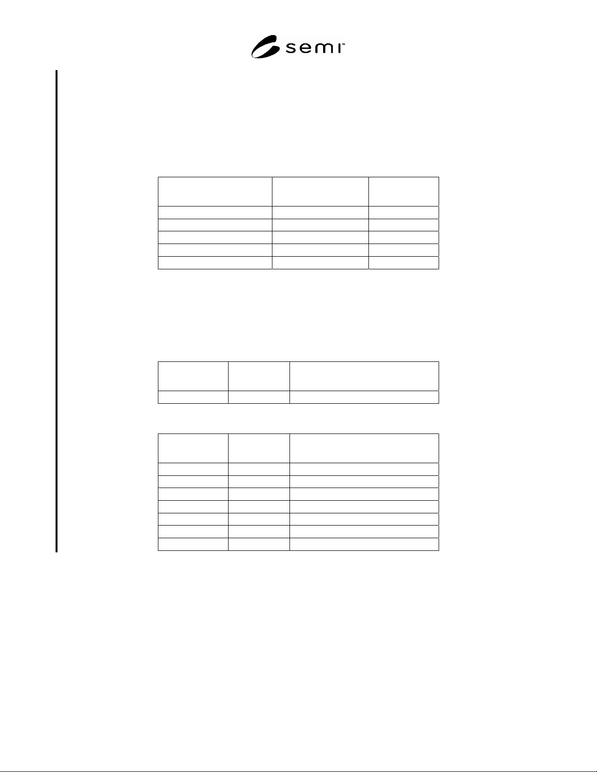
9.6.3.3 Table 35 shows the mapping of the SDM.
9.6.3.4 Objects specified in SEMI E54.11 are listed under the heading NCS Module reference. Every instance is
allocated to a slot number. The configuration can be modeled in the GSD by using the Module reference as key for
the module description.
9.6.3.5 The Sensor-BI-TH-EP can occur more than once. This shall be modeled in GSD in that way, that this
Module ID can be placed in several slots.
Table 35 Endpoint Device Object Identifiers
SDM Object
Name
SDM Object ID NCS Module
reference
Sensor-BI-TH-EP EPD3 203
Assembly-EPD#1 EPD4 204
Assembly- EPD#2 EPD5 205
Assembly- EPD#3 EPD6 206
Assembly- EPD#4 EPD7 207
9.6.4 Attributes
9.6.4.1 The mapping of Attribute Tags and Identifiers is defined in §7 for SAC. The same method applies here for
the SDM.
9.6.4.2 Tables 36 and 37 show the mapping of the specific SDM attributes.
Table 36 DM Object additional Attribute Identifiers
SEMI SDM
Attribute ID
PROFIBUS
Index
Attribute
SacA65 129 Number of Endpoint Objects
Table 37 Sensor-BI-TH-EP Object additional Attribute Identifiers
SEMI SDM
Attribute ID
PROFIBUS
Index
Attribute
EpA1 160 Minimum Time
EpA2 161 Maximum Time
EpA3 162 Target Time
EpA4 163 Elapsed Time
EpA5 164 Time Stamp
EpA6 165 Recipe Identifier
EpA7 166 Step Identifier
SEMI E54.8-0305 © SEMI 1999, 2005 21
9.6.5 Services
9.6.5.1 The mapping of Service Tags and Identifiers is defined in §7 for SAC. The same method applies here for
the SDM.
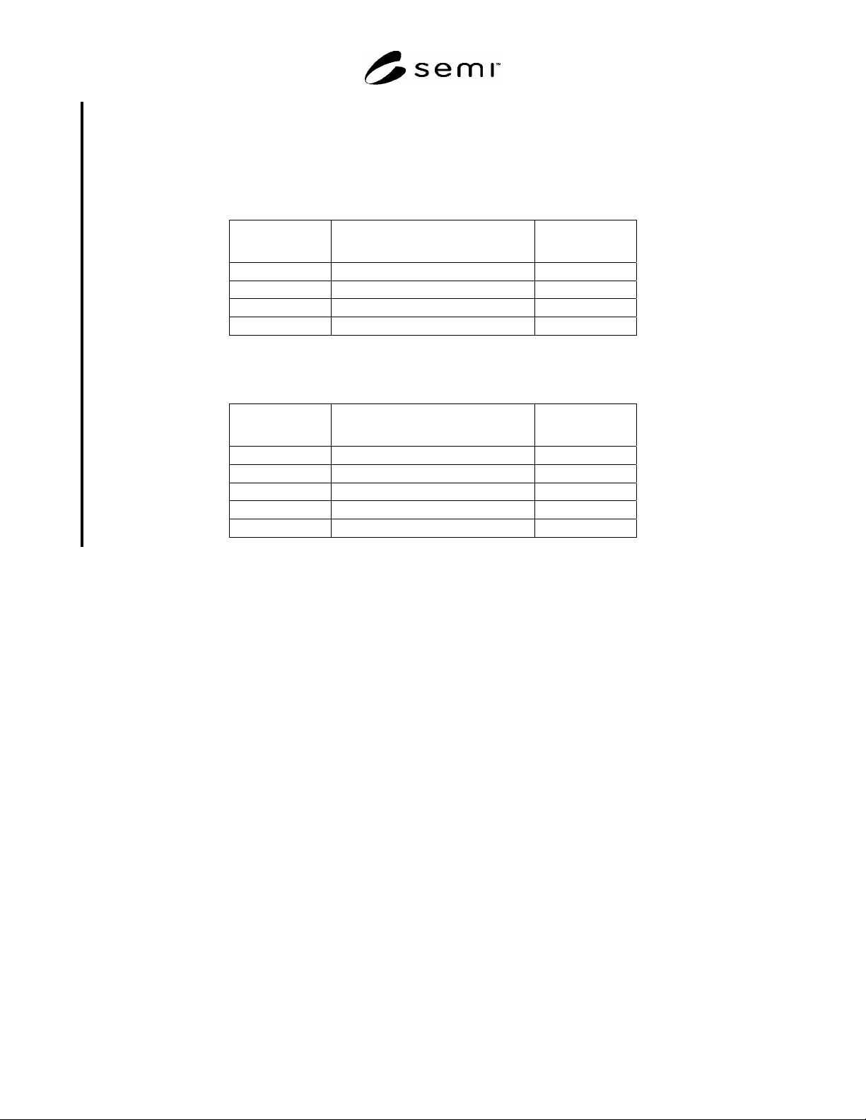
9.6.5.2 The additional Services of SAC are mapped as described in Table 38.
Table 38 SAC additional Service mapping
SEMI SDM Service
ID
Service Write Value to
Index 64
SacS33 Reset Endpoint 33
SacS34 Download Recipe 34
SacS35 Upload Recipe 35
SacS36 Calibrate 36
9.6.5.3 The additional Services of Sensor BI-EP are mapped as described in Table 39.
Table 39 Sensor BI-EP additional Service mapping
SEMI SDM Service
ID
Service Write Value to
Index 64
EpS1 Endpoint On 11
EpS2 Endpoint Off 12
EpS3 Endpoint Start 13
EpS4 Endpoint Suspend 14
EpS5 Endpoint Resume 15
NOTICE: SEMI makes no warranties or representations as to the suitability of the standards set forth herein for any
particular application. The determination of the suitability of the standard is solely the responsibility of the user.
Users are cautioned to refer to manufacturer’s instructions, product labels, product data sheets, and other relevant
literature respecting any materials mentioned herein. These standards are subject to change without notice.
The user’s attention is called to the possibility that compliance with this standard may require use of copyrighted
material or of an invention covered by patent rights. By publication of this standard, SEMI takes no position
respecting the validity of any patent rights or copyrights asserted in connection with any item mentioned in this
standard. Users of this standard are expressly advised that determination of any such patent rights or copyrights, and
the risk of infringement of such rights, are entirely their own responsibility.
Copyright by SEMI® (Semiconductor Equipment and Materials
International), 3081 Zanker Road, San Jose, CA 95134. Reproduction of
the contents in whole or in part is forbidden without express written
consent of SEMI.