semi合集-English.pdf - 第5468页
SEMI IN TERNA TIONA L STA N DA RDS MICROLI THOGRA P HY Sem iconduct or Equipm ent and Materials Inte rnational
SEMI PR9-0705 © SEMI 2005 11
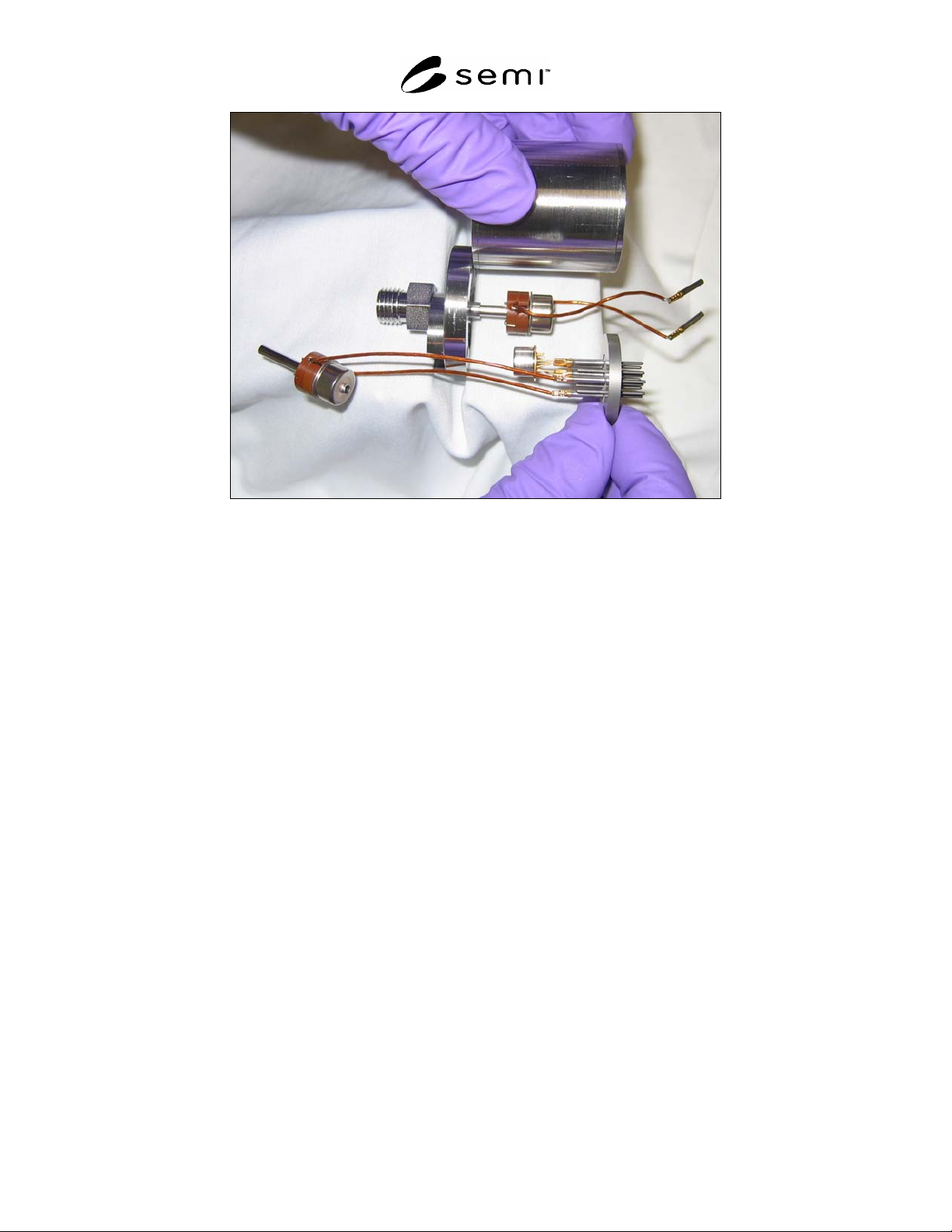
Figure 4
Microvalve in Fusion Reactor
9.5 Purpose — To be developed.
9.6 Scope — To be developed.
NOTICE: SEMI makes no warranties or representations as to the suitability of the standards set forth herein for any
particular application. The determination of the suitability of the standard is solely the responsibility of the user.
Users are cautioned to refer to manufacturer's instructions, product labels, product data sheets, and other relevant
literature, respecting any materials or equipment mentioned herein. These standards are subject to change without
notice.
By publication of this standard, Semiconductor Equipment and Materials International (SEMI) takes no position
respecting the validity of any patent rights or copyrights asserted in connection with any items mentioned in this
standard. Users of this standard are expressly advised that determination of any such patent rights or copyrights, and
the risk of infringement of such rights are entirely their own responsibility.
Copyright by SEMI® (Semiconductor Equipment and Materials
International), 3081 Zanker Road, San Jose, CA 95134. Reproduction of
the contents in whole or in part is forbidden without express written
consent of SEMI.

SEMI INTERNATIONAL STANDARDS
MICROLITHOGRAPHY
Semiconductor Equipment and Materials International

SEMI P1-1101 © SEMI 1981, 20011
SEMI P1-1101
SPECIFICATION FOR HARD SURFACE PHOTOMASK SUBSTRATES
This specification was technically approved by the Global Micropatterning Committee and is the direct
responsibility of the North American Micropatterning Committee. Current edition approved by the Japanese
Regional Standards Committee on August 3, 2001. Initially available at www.semi.org September 2001; to
be published November 2001. Originally published in 1981; previously published February 1999.
1 Purpose
1.1 This specification covers the general requirements
of the glass substrate for hard surface photomasks.
2 Scope
2.1 This document covers square photomasks up to 7
inches in length. 230 mm substrates are excluded from
this standard and can be found in SEMI P33.
2.2 This document also gives specifications for the
following materials:
• High Thermal Expansion (HTE),
• Medium Thermal Expansion (MTE),
• Low Thermal Expansion (LTE),
• Ultra Low Thermal Expansion (ULTE)
• Durable Fused Silica (DFS) glass for 193 nm
wavelength
• Modified Fused Silica (MFS) glass for 157 nm
wavelength.
2.3 This standard does not purport to address safety
issues, if any, associated with its use. It is the
responsibility of the users of this standard to establish
appropriate safety health practices and determine the
applicability or regulatory limitations prior to use.
3 Referenced Standards
3.1 SEMI Standards
SEMI P33 — Provisional Specification for Develop-
mental 230 mm Square Hard Surface Photomask
Substrates
3.2 ASTM Standards
1
ASTM E 228 — Test for Linear Thermal Expansion of
Rigid Solids with a Vitreous Silical Dilatometer
1 American Society for Testing and Materials, 100 Barr Harbor
Drive, West Conshohocken, Pennsylvania 19428-2959, USA.
Telephone: 610.832.9585, Fax: 610.832.9555 Website:
www.astm.org
3.3 ANSI/ASQC Standards
2
ANSI/ASQC Z1.4 — Sampling Procedures and Tables
for Inspection by Attributes
3.4 ISO Standard
3
ISO 14644-1 — Cleanrooms and Associated Controlled
Environments Part 1: Classification of Air Cleanliness
4 Terminology
4.1 Selected terms relating to photomasking are given
for information only in “Terms and Definitions
Relating to the Microlithography Industry” found at the
end of SEMI P33 “RELATED INFORMATION”.
Definitions may be found in what was ASTM F 127.
5 Ordering Information
5.1 Purchase orders for hard surface photomask
substrates furnished to this specification shall include
the following:
5.1.1 Nominal edge length, nominal thickness
dimension, and edge criteria (see Section 6);
5.1.2 Material (see Section 7);
5.1.3 Flatness quality area and flatness (Total Indicated
Reading, T.I.R.) see Section 8);
5.1.4 Visual quality area and defect limits (see Section
9); and
5.1.5 Lot acceptance criteria (see Section 10).
6 Dimensions and Permissible Variations
6.1 The square substrates shall conform to the
dimensional tolerances appropriate to the nominal edge
length and thickness as listed in Table 1. Dimensions
are illustrated in Figure 1 and a fixture for measuring
the diagonal dimensions is shown in Figure 2.
6.2 Substrates shall have chamfered or rounded edges.
The edges shall conform to the dimensional tolerances
2 American Society for Quality Control, 611 East Wisconsin
Avenue, Milwaukee, WI 53202, USA
3 International Organization for Standardization, ISO Central
Secretariat, 1, rue de Varembé, Case postale 56, CH-1211 Geneva 20,
Switzerland. Telephone: 41.22.749.01.11; Fax: 41.22.733.34.30
Website: www.iso.ch