semi合集-English.pdf - 第5896页
SEMI P38-1103 © SEMI 2002, 2003 8 Table 10 Optical Properties of Buffer Layer and Multilayer Stack Minimum multilayer stack refl ectivity at 150 < λ < 257 nm (See Note 2.) 55% Mean buffer layer reflectivity at 190&…
SEMI P38-1103 © SEMI 2002, 2003 7
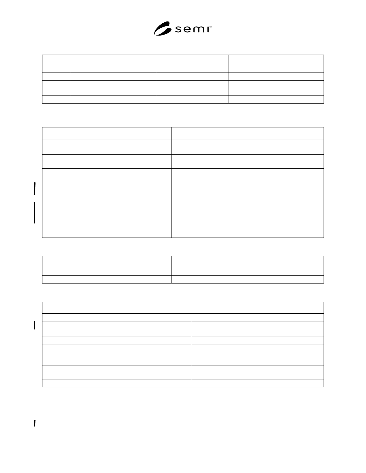
Table 6 Uniformity Of EUV Reflectivity Of Multilayer Stack
Class Maximum range of peak
reflectivity(absolute)
Maximum range of
bandwidth(nm at FWHM)
Maximum range of centroid wavelength
(nm)
A 0.50% 0.005 0.06
B 0.70% 0.005 0.08
C 0.80% 0.01 0.1
D 1.20% 0.01 0.12
Note 1: Mean is determined from measurements made at different spatial locations on the mask blank surface. Sample size and measurement
locations for determining range are to be agreed upon between user and supplier.
Table 7 Properties of Buffer Layer
Buffer layer properties Requirement
Buffer layer etch selectivity to multilayer Agreed upon between user and supplier
Buffer layer material composition Agreed upon between user and supplier
Focused ion beam etch selectivity between buffer layer
and absorber
Agreed upon between user and supplier
Focused ion beam etch selectivity between buffer layer
and multilayer
Agreed upon between user and supplier
Secondary electron contrast of the buffer layer surface
with respect to the surface of the absorber layer(s) for
between 0.5 and 2 kV primary electrons
Agreed upon between user and supplier
Secondary electron contrast of the buffer layer surface
with respect to the surface of the capping layer(s) for
between 0.5 and 2 kV primary electrons
Agreed upon between user and supplier
Buffer etch selectivity to absorber stack Agreed upon between user and supplier
Buffer layer thickness Agreed upon between user and supplier
Table 8 Properties Of Absorber Layer or Layers
Absorber layer properties Requirement
Material composition of absorber layer(s) Agreed upon between user and supplier
Thickness of absorber layer(s) Agreed upon between user and supplier
Table 9 Properties Of Absorber Stack
Attribute Requirement
Stress −200 to 200 MPa
Mean reflectivity at EUV wavelength (See Note 1 and 2.) < 0.5%
Uniformity of EUV reflectivity < 0.1% TIR
Thickness uniformity Agreed upon between user and supplier
Etch rate in cleaning solutions (See Note 3.) Agreed upon between user and supplier
Thickness change after 50 billion pulses in EUV exposure tool (See
Note 4.)
< 1 nm
Stress change after 50 billion pulses in EUV exposure tool (See
Note 4.)
< 50 MPa
Absorber stack outgassing during EUV radiation (See Note 4.) Agreed upon between user and supplier
Note 1: Mean is determined from measurements made at different spatial locations on the mask blank surface. Sample size and measurement
locations for determining range are to be agreed upon between user and supplier.
Note 2: Reflectivity at 6 degrees angle of incidence with respect to the normal to the absorber surface at the mean median reflected wavelength
specified in Table 4 and integrated over the bandwidth equal to the FWHM of the reflectivity versus EUV wavelength.
Note 3: Cleaning solutions to be agreed upon between user and supplier.
Note 4: ≥ 1 mJ/cm
2
/pulse in a bandwidth that equals 2% of the nominal wavelength full width at half maximum (FWHM).
SEMI P38-1103 © SEMI 2002, 2003 8
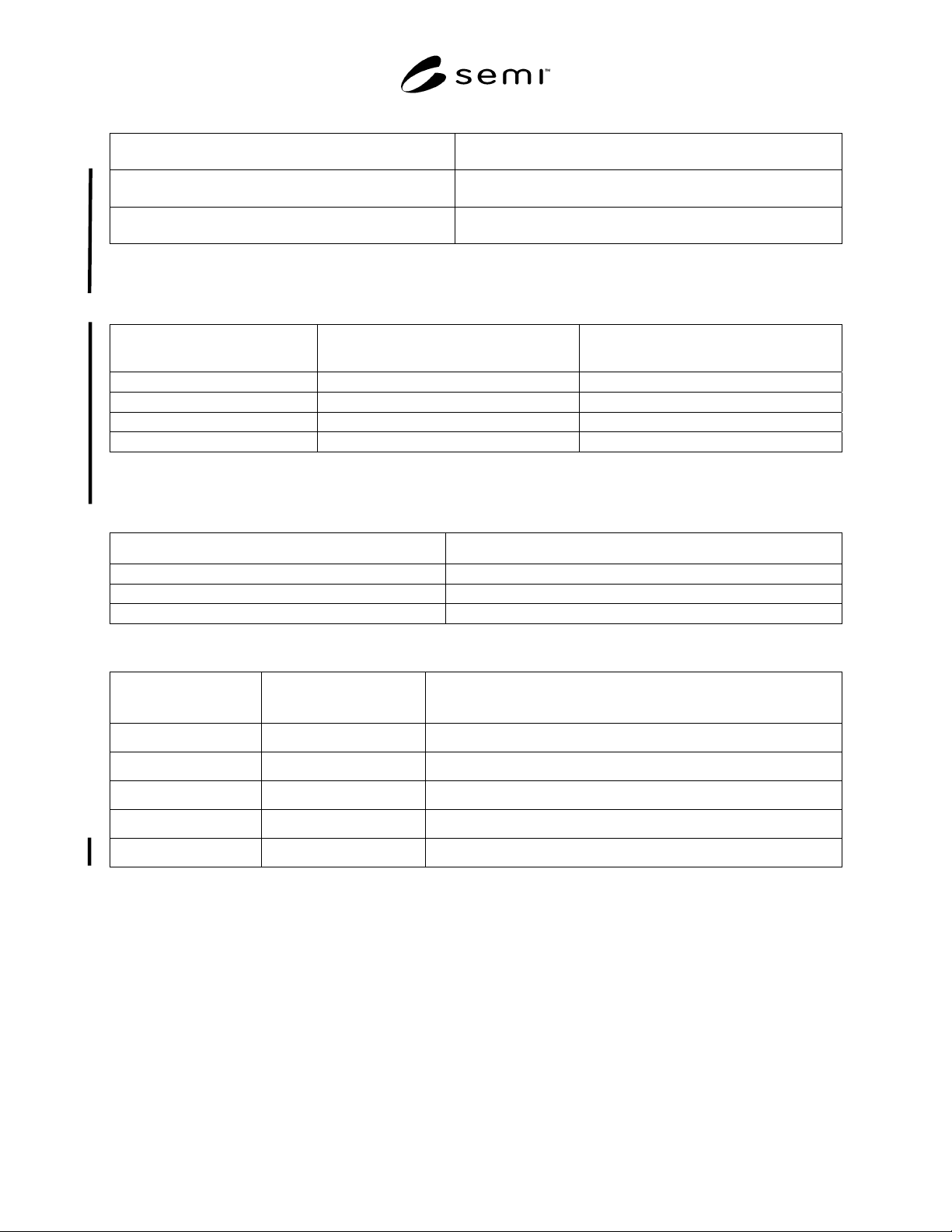
Table 10 Optical Properties of Buffer Layer and Multilayer Stack
Minimum multilayer stack reflectivity at 150 < λ< 257 nm
(See Note 2.)
55%
Mean buffer layer reflectivity at 190<λ<257 nm (See Notes
1 and 2.)
Agreed upon between user and supplier
Uniformity of buffer layer reflectivity (absolute) (See Note
1.)
Agreed upon between user and supplier
Note 1: Mean is determined from measurements made at different spatial locations on the buffer layer or multilayer stack surface. Sample size
and measurement locations for determining range are to be agreed upon between user and supplier.
Note 2: λ is the inspection wavelength. Reflectivity is specified for < 1% fractional bandwidth at normal incidence
Table 11 Optical Properties of Absorber Stack Surface
Class Mean absorber stack reflectivity at
190<
λ
<257 nm (See Notes 1 and 2.)
Uniformity of reflectivity (absolute)
(See Notes 1 and 2.)
A 5% ± 2%
B 10% ± 1.5%
C 15% ± 1.5%
D 20% ± 1.5%
Note 1: Mean is determined from measurements made at different spatial locations on the absorber stack surface. Sample size and measurement
locations for determining range are to be agreed upon between user and supplier.
Note 2: λ is the inspection wavelength. Reflectivity is specified for < 1% fractional bandwidth and at normal incidence.
Table 12 Properties of the Conductive Layer on the Back Side of the Mask Substrate
Conductive layer properties Requirement
Thickness Agreed upon between user and supplier
Stress Agreed upon between user and supplier
Mechanical durability Agreed upon between user and supplier
Table 13 Defect Requirements for Multilayer Stack
Class PSL equivalent size range
(nm) (See Note 1.)
Maximum defect count
A > 25 0
B > 30 0
C > 40 0
D (Test) > 60 Agreed upon between user and supplier
E (Test) > 90 Agreed upon between user and supplier
Note 1: PSL equivalent size means the detected defect appears to be the same size as a polystyrene latex sphere examined under the same
inspection conditions. Defect count for defects with size smaller than that shown is not specified.
SEMI P38-1103 © SEMI 2002, 2003 9
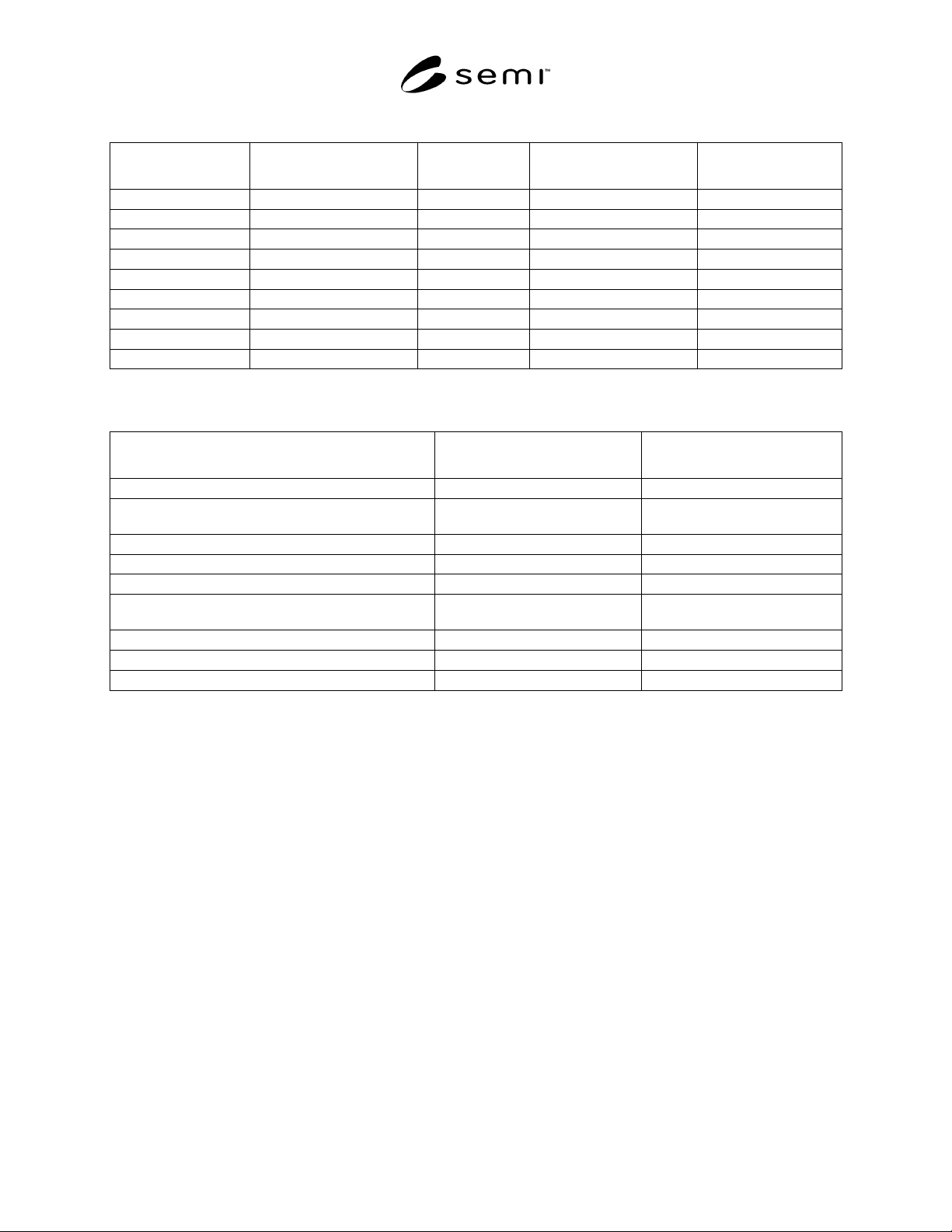
Table 14 Defect Requirements for Absorber Stack
Class Defect size range (nm) (See
Note 1.)
Maximum count Defect size range (nm) (See
Note 1)
Maximum count
A1 15–180 0 > 180 0
A2 15–180 10 > 180 0
B1 25–265 0 > 265 0
B2 25–265 10 > 265 0
C1 35–360 0 > 360 0
C2 35–360 10 > 360 0
D1 50–520 0 > 520 0
D2 50–520 10 > 520 0
E (Test) < 1000 1500 > 1000 0
Note 1: PSL equivalent size means the detected defect appears to be the same size as a polystyrene latex sphere examined under the same
inspection conditions. Defect count for defects with size smaller than that shown is not specified.
Table 15 Items Included In Mask Blank Label
Item in label Corresponding Table or Figure Included in label for Type 1 (See
Note 1)
Type Table 1 Yes
Layer quality area dimensions, W
L
followed by D
L
(to
nearest 0.1 mm)
Figure 2 Yes
Mean median wavelength (to nearest 0.01 nm) Table 4 Yes
Peak reflectivity class of multilayer stack Table 5 Yes
Multilayer stack reflectivity uniformity class Table 6 Yes
Defect quality area dimensions, W
L
followed by D
L
(to nearest 0.1 mm)
Figure 3 Yes
Multilayer stack defect class Table 13 Yes
Class for absorber optical properties Table 11 No
Absorber defect class Table 14 No
Note 1: All items in Table 15 are included in the label for mask blank types 2 and 3.
NOTICE: SEMI makes no warranties or representations as to the suitability of the standards set forth herein for any
particular application. The determination of the suitability of the standard is solely the responsibility of the user.
Users are cautioned to refer to manufacturer's instructions, product labels, product data sheets, and other relevant
literature, respecting any materials or equipment mentioned herein. These standards are subject to change without
notice.
By publication of this standard, Semiconductor Equipment and Materials International (SEMI) takes no position
respecting the validity of any patent rights or copyrights asserted in connection with any items mentioned in this
standard. Users of this standard are expressly advised that determination of any such patent rights or copyrights, and
the risk of infringement of such rights are entirely their own responsibility.
Copyright by SEMI® (Semiconductor Equipment and Materials
International), 3081 Zanker Road, San Jose, CA 95134. Reproduction o
f
the contents in whole or in part is forbidden without express written
consent of SEMI.