semi合集-English.pdf - 第7576页
SEMI MF1982-1103 © SEMI 2003 7 w c c b s S W A A A TO 1 × × − = (5) where: TO = total organic cont aminants, ng C 16 (n-C 16 H 34 ) equivalent/ cm 2 , A s = total area integr ated from GC-MS chromato- gram of the sa mple…

SEMI MF1982-1103 © SEMI 2003 6
(phosphorus selective detector) chromatogram of the
sample wafer. Obtain total area of the blank wafer (A
b
)
by summing up all the peak areas integrated from GC-
(phosphorus selective detector) chromatogram of the
blank wafer. Obtain the area of the standard peak (A
p
)
integrated from GC-(phosphorus selective detector)
chromatogram of the standard sample.
8 Calculation
8.1 Method A
8.1.1 Calculation of Total Organic Contaminants
8.1.1.1 When AED or FID is used:
16
1
1002.6
10
23
9
×
×
×××
×
×
−
=
−
FSMW
W
A
AA
TC
wc
c
c
bs
(1)
where:
TC = total organic carbon, C atoms/cm
2
,
A
s
= total area integrated from GC-AED or FID
chromatogram of the sample wafer for carbon
compounds,
A
b
= total area integrated from GC-AED or FID
chromatogram of the blank wafer,
A
c
= total area integrated from GC-AED or FID
chromatogram of the standard peak,
W
c
= weight of C
16
standard injected onto the stan-
dard tube, ng,
MW
c
= molecular weight of n-C
16
H
34
= 226.45,
S
w
= total area of the wafer sample, cm
2
,
F =
conversion factor = (W
T
− W
U
)/W
T
,
W
T
= total weight of the wafer, g, and
W
U
= weight of unused part of the wafer, g.
NOTE 5: In this calculation, blank subtraction (−A
b
) is
optional.
8.1.1.2 When MS is used:
FS
W
A
AA
TO
w
c
c
bs
×
××
−
=
1
(2)
where:
TO = total organic contaminants, ng C
16
(n-C
16
H
34
)
equivalent/cm
2
,
A
s
= total area integrated from GC-MS chromato-
gram of the sample wafer,
A
b
= total area integrated from GC-MS chromato-
gram of the blank wafer,
A
c
= total area integrated from GC-MS chroma-
togram of the standard peak,
W
c
= weight of C
16
standard injected onto the stan-
dard tube, ng,
S
w
= total area of the wafer sample, cm
2
,
F =
conversion factor = (W
T
− W
U
)/W
T
,
W
T
= total weight of wafer, g, and
W
U
= weight of unused part of the wafer, g.
See Note 5.
NOTE 6: Recommended mass range to be scanned is 33 to
700 amu.
8.1.2 Calculation of Total Organophosphorus (TP):
FSMW
W
A
AA
TP
wp
p
p
bs
×
×××
×
×
−
=
−
1
1002.6
10
23
9
(3)
where:
TP = total organophosphorus, P atoms/cm
2
,
A
s
= total area integrated from GC-(phosphorus
selective detector) chromatogram of the sample
wafer for phosphorus compounds only,
A
b
= total area integrated from GC-(phosphorus
selective detector) chromatogram of the blan
k
wafer,
A
p
= total area integrated from GC-(phosphorus
selective detector) chromatogram of the
standard peak,
W
p
= weight of phosphorus standard (TCEP or TBP)
injected onto the standard tube, ng,
MW
p
= molecular weight of phosphorus standard
(TCEP = 285.49, or TBP = 266.3),
S
W
= total area of the wafer sample, cm
2
,
F =
conversion factor = (W
T
− W
U
)/W
T,
W
T
= total weight of the wafer, g, and
W
U
= weight of unused part of the wafer, g.
See Note 5.
8.2 Method B
8.2.1 Calculation of Total Organic Contaminants
8.2.1.1 When AED or FID is used:
16
1
1002.6
10
23
9
××××
×
×
−
=
−
wc
c
c
bs
SMW
W
A
AA
TC
(4)
where:
TC = total organic carbon, C atoms/cm
2
,
A
s
= total area integrated from GC-AED or FID,
chromatogram of the sample wafer for carbon
compounds,
A
b
= total area integrated from GC-AED or FID
chromatogram of the blank wafer,
A
c
= total area integrated from GC-AED or FID
chromatogram of the standard peak,
W
c
= weight of C
16
standard injected onto the
standard wafer, ng,
MW
c
= molecular weight of n-C
16
H
34
= 226.45,
S
w
= one side area of the wafer sample, cm
2
.
See Note 5.
8.2.1.2 When MS is used:

SEMI MF1982-1103 © SEMI 2003 7
w
c
c
bs
S
W
A
AA
TO
1
××
−
= (5)
where:
TO = total organic contaminants, ng C
16
(n-C
16
H
34
)
equivalent/cm
2
,
A
s
= total area integrated from GC-MS chromato-
gram of the sample wafer,
A
b
= total area integrated from GC-MS chromato-
gram of the blank wafer,
A
c
= total area integrated from GC-MS chromato-
gram of the standard peak,
W
c
= weight of C
16
standard injected onto the wafer,
ng,
S
w
= one side area of the wafer sample, cm
2
.
See Notes 5 and 6.
8.2.2 Calculation of Total Organophosphorus (TP):
wp
p
p
bs
SMW
W
A
AA
TP
1
1002.6
10
23
9
×××
×
×
−
=
−
(6)
where:
TP = total organophosphorus, P atoms/cm
2
,
A
s
= total area integrated from GC-(phosphorus
selective detector) chromatogram of the sample
wafer for phosphorus compounds only,
A
b
= total area integrated from GC-(phosphorus
selective detector) chromatogram of the blan
k
wafer,
A
p
= total area integrated from GC-(phosphorus
selective detector) chromatogram of the
standard peak,
W
p
= weight of phosphorus standard (TCEP or TBP)
injected onto the wafer, ng,
MW
p
= molecular weight of phosphorus standard
(TCEP = 285.49 or TBP = 266.3),
S
W
= area of one surface of the wafer sample, cm
2
.
See Note 5.
9 Report
9.1 Report the following information:
9.1.1 Sample identification, sample size, sample
history including how received or packaged if it has
been shipped, side of wafer desorbed (front, back, or
both). (Shipping often can add or remove organic
compounds). If the wafer is a witness wafer, report
how prepared and exposure conditions, location
whether horizontal or vertical, time, flow, etc.
9.1.2 Analysis date, analysis method, wafer desorption
time and temperature, purge gas used.
9.1.3 Manufacturer, types, and models of instruments.
9.1.4 Identification of operator.
9.1.5 Testing laboratory.
9.1.6 Software version of instrument.
9.1.7 Analysis results.
9.1.7.1 Total organic contaminants, C atoms/cm
2
(when AED or FID is used), or ng C
16
(n-C
16
H
34
)
equivalent/cm
2
(when MS is used).
9.1.7.2 Total organophosphorus, P atoms/cm
2
.
9.1.8 Blank wafer data. The blank wafer should be
treated with the same desorption procedure as the
sample wafers.
9.1.9 Calibration data.
10 Precision and Bias
10.1 Precision — The precision of these test methods
can be determined from the reproducibility measure-
ment of standards. The accuracy of these test methods
can be measured from the recoveries of standards.
10.2 Bias — Bias for these test methods has not been
determined.
11 Keywords
11.1 atomic emission detector (AED); flame ionization
detector (FID); flame photometric detector (FPD); gas
chromatography; mass spectrometer (MS);
nitrogen/phosphorus thermionic ionization detector
(NPD); organic contamination; organophosphorus
compounds; phosphorus selective detector; silicon
wafer surfaces; thermal desorption
SEMI MF1982-1103 © SEMI 2003 8
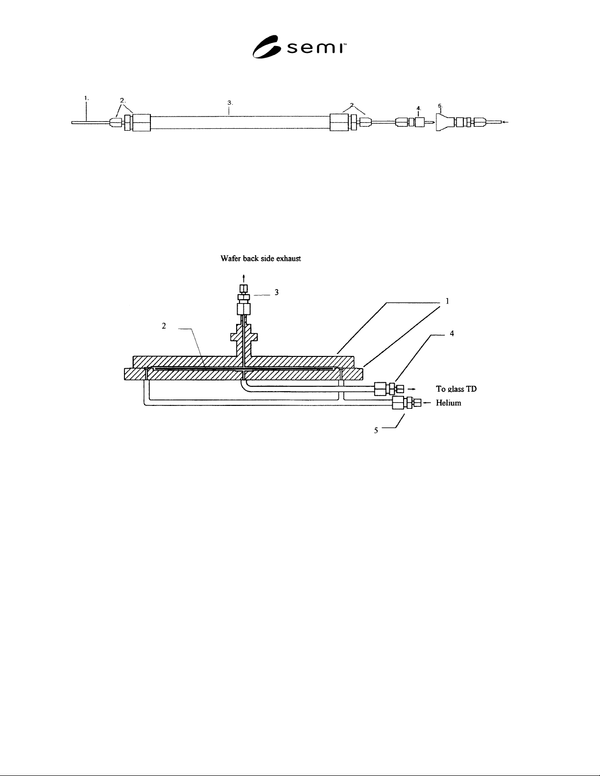
1. Sample thermal desorption tube
2. Fitting
3. Wafer desorption oven
4. Quick connect male end
5. Quick connect female end
Figure 1
Schematic of Wafer Desorption Setup
1. Quartz chamber
2. Silicon wafer
3. Fitting
4. Fitting
5. Fitting
Figure 2
Schematic of Quartz Chamber
NOTICE: SEMI makes no warranties or representations as to the suitability of the standards set forth herein for any
particular application. The determination of the suitability of the standard is solely the responsibility of the user.
Users are cautioned to refer to manufacturer's instructions, product labels, product data sheets, and other relevant
literature, respecting any materials or equipment mentioned herein. These standards are subject to change without
notice.
By publication of this standard, Semiconductor Equipment and Materials International (SEMI) takes no position
respecting the validity of any patent rights or copyrights asserted in connection with any items mentioned in this
standard. Users of this standard are expressly advised that determination of any such patent rights or copyrights, and
the risk of infringement of such rights are entirely their own responsibility.
nitrogen
gas
Copyright by SEMI® (Semiconductor Equipment and Materials
International), 3081 Zanker Road, San Jose, CA 95134. Reproduction o
f
the contents in whole or in part is forbidden without express written
consent of SEMI.