semi合集-English.pdf - 第5341页
SEMI M52-0703 © SEMI 2002, 2003 5 5.3.9 level 1 variability ( σ 1 ) — the variation of measurement results obtained by repeated measurements with the sam e test specimen(s) and the same measurem ent tool under nominal ly…

SEMI M52-0703 © SEMI 2002, 2003 4
5.2.2 dimple — a shallow depression with gently
sloping sides that exhibits a concave, spherical shape
and is visible to the unaided eye under proper lighting
conditions. [SEMI M1]
5.2.3 haze — non-localized light scattering resulting
from surface topography (microroughness) or from
dense concentrations of surface or near surface
imperfections. [SEMI M1]
5.2.4 mound (epitaxial wafer) — regularly shaped
bump on a semiconductor wafer surface, which may
have one or more irregularly developed facets. [ASTM
F 1241]
5.2.5 mound (polished wafer) — a defect characterized
by small circular raised areas on the surface, typically
0.1 to 1.0 µm in height, 5 to 25 mm in diameter and
located in random positions on the wafer.
5.2.6 particle — a small, discrete piece of foreign
material or silicon not connected crystallographically to
the wafer. [SEMI M1]
5.2.7 pit — a depression in a wafer surface that has
steeply sloped sides that meet the surface in a
distinguishable manner in contrast to the rounded sides
of a dimple. [SEMATECH Technology Transfer
95082941A-TR]
5.2.8 scratch —
a shallow groove or cut below the
established plane of the wafer surface, with a length to
width ratio greater than 5:1. [SEMATECH Technology
Transfer 95082941A-TR
5.2.9 slip — a process of plastic deformation in which
one part of a crystal undergoes a shear displacement
relative to another in a fashion that preserves the
crystallinity of the material. [ASTM F 1241]
5.2.10 slurry ring — a ring-shaped area, higher than
the surrounding wafer surface caused by incomplete
cleaning of slurry residue.
5.2.11 spike — in an epitaxial wafer, a tall thin
dendrite of crystalline filament that often occurs at the
center of a recess. [ASTM F 1241, see also ASTM F
154]
5.2.12 stacking fault —
a two dimensional defect that
results from a deviation from the normal stacking
sequence of atoms in a crystal. [ASTM F 1241, see also
ASTM F 154]
5.2.13 stain — area contamination that is chemical in
nature and cannot be removed except through further
lapping or polishing. [ASTM F 1241]
5.3 Other Terminology
5.3.1 bias — the difference between the average of
measurements made on the same object and its true
value. Sufficient measurements are needed to mitigate
the effects of variability. [SEMI E89]
5.3.2 calibration — a measurement process that
assigns a value to the property of an artifact or to the
response of an instrument relative to reference
standards or to a designated measurement process.
5.3.2.1 Discussion — The purpose of calibration is to
eliminate or reduce bias in the user’s measurement
system relative to the reference base. The calibration
process compares an unknown or test item or
instrument with reference standards according to a
specific algorithm, often in the form of a specific
calibration curve. [SEMI
E89]
5.3.3 capture rate — the probability that an SSIS
detects an LLS of latex sphere equivalent (LSE) signal
value at some specified SSIS operational setting.
5.3.4 classification accuracy — how many of a
particular defect population are correctly classified.
5.3.4.1 Discussion — The accuracy of a classification
system is expressed as an equation: Accuracy = A/H,
where A is the total quantity of correctly classified
defects (human and machine classification results
agree) and H is the total quantity of human classified
defects.
5.3.5 classification purity — how many of the defects
classified by machine (SSIS) are properly classified.
5.3.5.1 Discussion — The purity of a classification
system can be expressed as an equation: Purity = A/M,
where A is the total quantity of correctly classified
defects (human and machine classification results
agree) and M is the total quantity of defects classified
as a specific class by machine (SSIS).
5.3.6 compatibility — the capability of measurement
equipment to emulate the measurement process of other
tools. Downward compatibility refers to former
generation(s) of the same or similar type of equipment
of an equipment supplier.
5.3.7 correlation — the relation of measurement
results obtained by repeated measurements with the
same set of test specimen(s) and any two measurement
tools expressed in terms of a regression curve.
5.3.8 CRM (Certified Reference Material) — reference
material, accompanied by a certificate, one or more of
whose property values are certified by a procedure
which establishes its traceability to an accurate
realization of the unit in which the property values are
expressed, and for which each certified value is
accompanied by an uncertainty at a stated level of
confidence. [ISO Guide 30:1992]

SEMI M52-0703 © SEMI 2002, 2003 5
5.3.9 level 1 variability (σ
1
) — the variation of
measurement results obtained by repeated
measurements with the same test specimen(s) and the
same measurement tool under nominally identical
conditions without replacing the test specimen between
subsequent measurement runs.
σ
1
tests are performed
with a single calibration in the shortest possible time
interval.
5.3.10 level 2 variability (σ
2
) — the variation of
measurement results obtained by repeated
measurements with the same test specimen(s) and the
same measurement tool with replacing the test
specimen between subsequent measurement runs but
otherwise under nominally identical conditions. σ
2
tests are performed with a single calibration in the
shortest possible time interval.
5.3.11 level 3 variability (σ
3
) — the variation of
measurement results obtained by repeated
measurements with the same test specimen(s) and the
same measurement tool with replacing the test
specimen between subsequent measurement runs but
otherwise under nominally identical conditions. σ
3
tests
are performed over a time period greater than σ
2
tests
without operator induced adjustment.
5.3.12 matching tolerance (∆
m
) — the difference in
bias for any two measurement tools of the same kind.
Otherwise matching tolerance tests are performed under
the conditions of σ
3
tests.
5.3.13 scanning surface inspection system (SSIS) — An
instrument for rapid examination of the entire quality
area on a wafer to detect the presence of localized light
scatterers or haze or both; also called particle counter
and laser surface scanner.
5.3.14 sorting — real and virtual separation of test
specimens in different categories specified by one or
multiple parameters.
6 Recommended Specification for
Measurement Equipment for Silicon Wafers of
the 130-nm Technology Generation
6.1 The recommended specification is structured in
three sections (Tables 1–3):
• Generic Equipment Characteristics (Table 1)
• Materials to be measured (Table 2)
• Metrology Specific Equipment Characteristics
(Table 3)
6.1.1 Tables 1–3 contain the recommended
specifications, referenced documents, test methods, and
comments. Additional explanations and discussions are
provided in this section.
6.2 Generic Equipment Characteristics (Table 1)
6.2.1 The section “Generic Equipment Characteristics”
consists of five subsections:
• Wafer handling
• Reliability
• Procedural
• Documentation
• Computer/User Interface/Connectivity
6.2.2 Subsections covering “Facilities Requirements”
and “Safety/Legal/Regulatory” are not included in the
present guide as these issues are highly user specific
and dependent on national regulations.
6.3 Materials to be measured (Table 2)
6.3.1 Table 2 specifies the parameters of silicon wafers
that the measurement equipment must be capable to
handle and to measure.
6.4 Metrology Specific Equipment Characteristics
(Table 3)
6.4.1 This section specifies the measurement functions
of the SSIS, the setup parameters of the SSIS and the
performance of the SSIS. Specifications in Table 3
apply to wafer front side surface inspection only.
6.4.1.1 For back surface inspection, particles,
scratches, and haze are required to be detected.
6.4.2 The surface defects to be detected by the SSIS
are listed in Table 3, lines 1.1.1 to 1.1.14. They are
reported as LLS or XLS. The measurement
performance of the equipment is verified with PSL
sphere depositions on wafers that meet the COP and
haze requirements of the 130-nm technology
generation.
6.4.3 All size units of LLS are given in [length unit]
LSE, e.g., nm LSE, and refer to a nominal diameter.
6.4.4 The geometrical size of a defect (LLS) may differ
considerably from its size as reported in LSE units, as
the cross section for light scattering of a defect depends
sensitively on the properties of the LLS.
6.4.5 PSL depositions used as reference materials are
required to be CRMs, traceable to a National Standards
Laboratory.
6.4.6 For COPs and particles, classification accuracy
and purity are specified.
SEMI M52-0703 © SEMI 2002, 2003 6
6.4.7 In this guide, a hierarchy of variability levels is used to describe the performance of measurement equipment
that is calibrated and adjusted/aligned according to the supplier's procedures. The various terms are defined in
Section 5. These variability levels are consistent with terms defined in SEMI E89 but not fully interchangeable.
Their relation is indicated in parentheses.
6.4.7.1 Level 1 variability: standard deviation σ
1
(SEMI E89 static repeatability)
6.4.7.2 Level 2 variability: standard deviation σ
2
(SEMI E89 dynamic repeatability)
6.4.7.3 Level 3 variability: standard deviation σ
3
(SEMI E89 reproducibility)
6.4.7.4 In addition two levels of systematic off-set between different tools are defined:
6.4.7.5 Matching tolerance (difference of means ∆
m
)
6.4.7.6 Correlation (regression curve)
6.4.8 Explicitly specified in the present guide is mainly level 3 variability and matching tolerance.
6.4.9 For SSIS, downward compatibility is subject to limitations imposed by changes in geometry and number of
detectors.
6.4.10 For sizing calibration, deposition CRMs are available from a variety of sources. On the other hand, a
reference standard for the defect coordinate performance is not available.
7 Related Documents
7.1 Glossary of Terms Related to Particle Counting and Surface Microroughness of Silicon Wafers,
SEMATECH
Technology Transfer 95082941A-TR
8
7.2 International Technology Roadmap for Semiconductors: 1999 edition
1
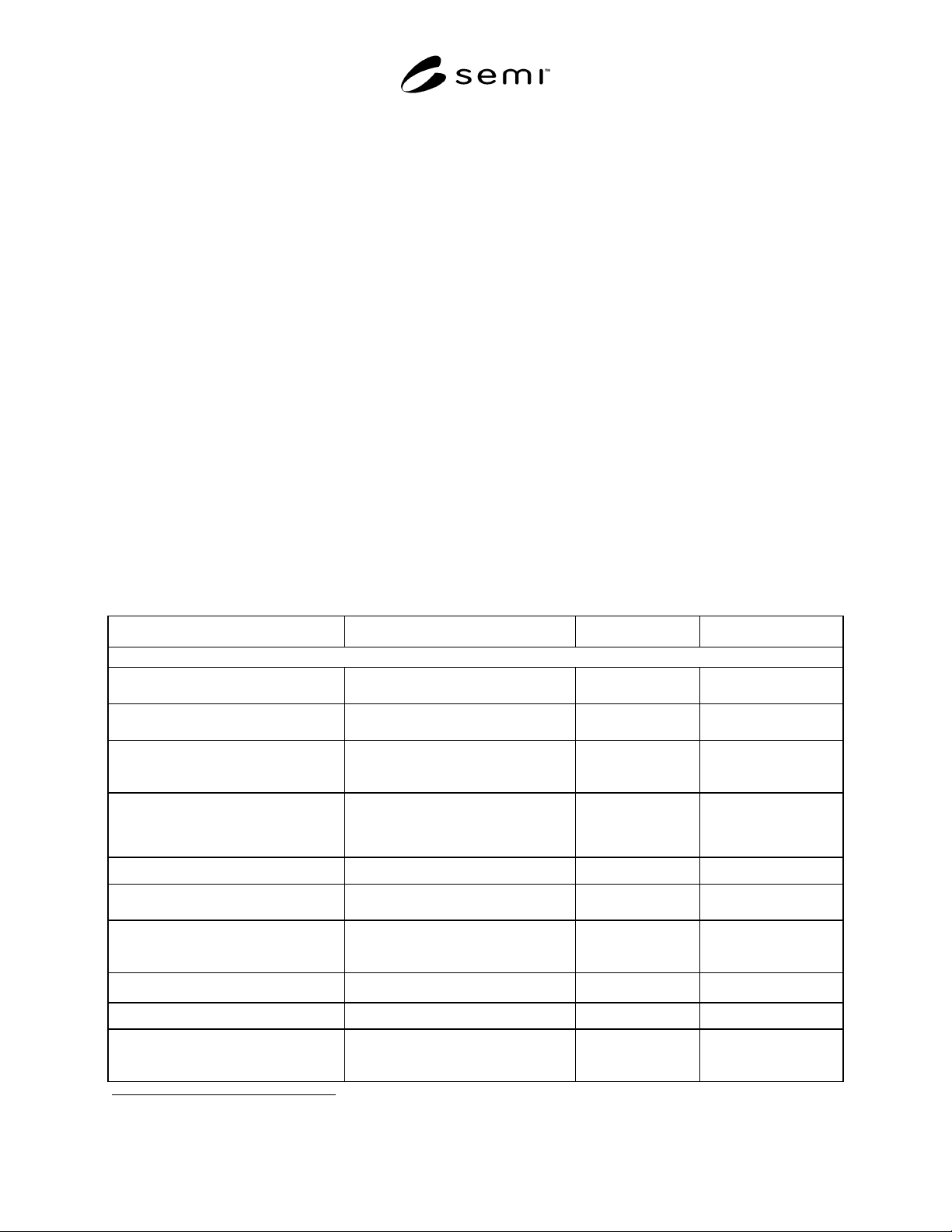
Table 1 Generic Equipment Characteristics
Item Recommended Specification Comment References
1 WAFER HANDLING
1.1 Robot End-Effector
optional wafer edge or backside contact edge as defined by
SEMI M1
1.2 Scan Stage
optional wafer edge or backside contact edge as defined by
SEMI M1
1.3 Wafer Contact Materials
contact materials to leave metals and
organics on wafers less than as defined
in ITRS 99.
1.4 Wafer Detection
protection of accidental contact due to
e.g. cross-slotting double slotting, etc.
1.5 Wafer Rotational Alignment
random in, aligned out
1.6 Number of Cassette Stations
2-4, arbitrary sender/receiver
assignment
1.7 Type of Cassettes
open, FOUP/SMIF, FOSB to be specified
alternatively
SEMI E1.9, SEMI E19,
SEMI E47, SEMI
E47.1, SEMI M31
1.8 Cassette Loading
manual/guided vehicle, conveyor belt
1.9 Automatic Cassette ID
user specific
1.10 Wafer Seating
vertical or off-horizontal during setting
cassette on station
by operator
8 International SEMATECH, 2706 Montopolis Drive, Austin, TX 78741-6499, USA Website: www.sematech.org