semi合集-English.pdf - 第6361页
SEMI G70-0996 © SEMI 1996, 2004 2 4.1.2 coil set — longitudinal bowing of the leadfram e strip length (see Figure 2). Figure 2 Coil Set 4.1.3 coined dept h — the diffe rence in height between the top surface of the coine…
1 SEMI G70-0996 © SEMI 1996, 2004
SEMI G70-0996 (Reapproved 1104)
STANDARD FOR EQUIPMENT AND LEADFRAME FIXTURES FOR
MEASUREMENT OF PLASTIC PACKAGE LEADFRAMES
This standard was technically approved by the Global Assembly & Packaging Committee and is the direct
responsibility of the Japanese Packaging Committee. Current edition approved by the Japanese Regional
Standards Committee on July 23, 2004. Initially available at www.semi.org September 2004; to be published
November 2004. Originally published in 1996.
1 Purpose
1.1 This standard describes the equipment and
leadframe fixtures used for measurement of Z-axis
dimensions of plastic package leadframes.
2 Scope
2.1 This standard mainly describes the equipment and
leadframe fixture for measurement of leadframes that
are 0.15 mm in thickness as used for TSOP and TQFP
packages listed in group II in Table 1.
2.2 This standard also may be applied for leadframe of
conventional packages which are 0.2 mm in
thickness.
Table 1 Package Classification
Group I Group II
SSOP
DIP TSOP
ZIP TSSOP
SOJ QFP
SOP TQFP
QFJ (PLCC) LQFP
SVP
NOTE 1: Packages should be classified by EIAJ and JEDEC
specifications.
NOTICE: This standard does not purport to address
safety issues, if any, associated with its use. It is the
responsibility of the users of this standard to establish
appropriate safety and health practices and determine
the applicability of regulatory or other limitations prior
to use.
3 Referenced Standards
3.1 SEMI Standard
SEMI G57 — Guideline for Standardization of
Leadframe Terminology
3.2 EIAJ Standard
1
ED-7411 — General Rules for the Preparation of
Outline Drawings of Integrated Circuits, Packages
Name and Code
3.3 JEDEC Specifications
2
Pub. No. 95 — Registered and Standard Outlines for
Semiconductor Devices
NOTICE: Unless otherwise indicated, all documents
cited shall be the latest published versions.
4 Terminology
4.1 Definitions
NOTE 2: See SEMI G57 for leadframe features terminology.
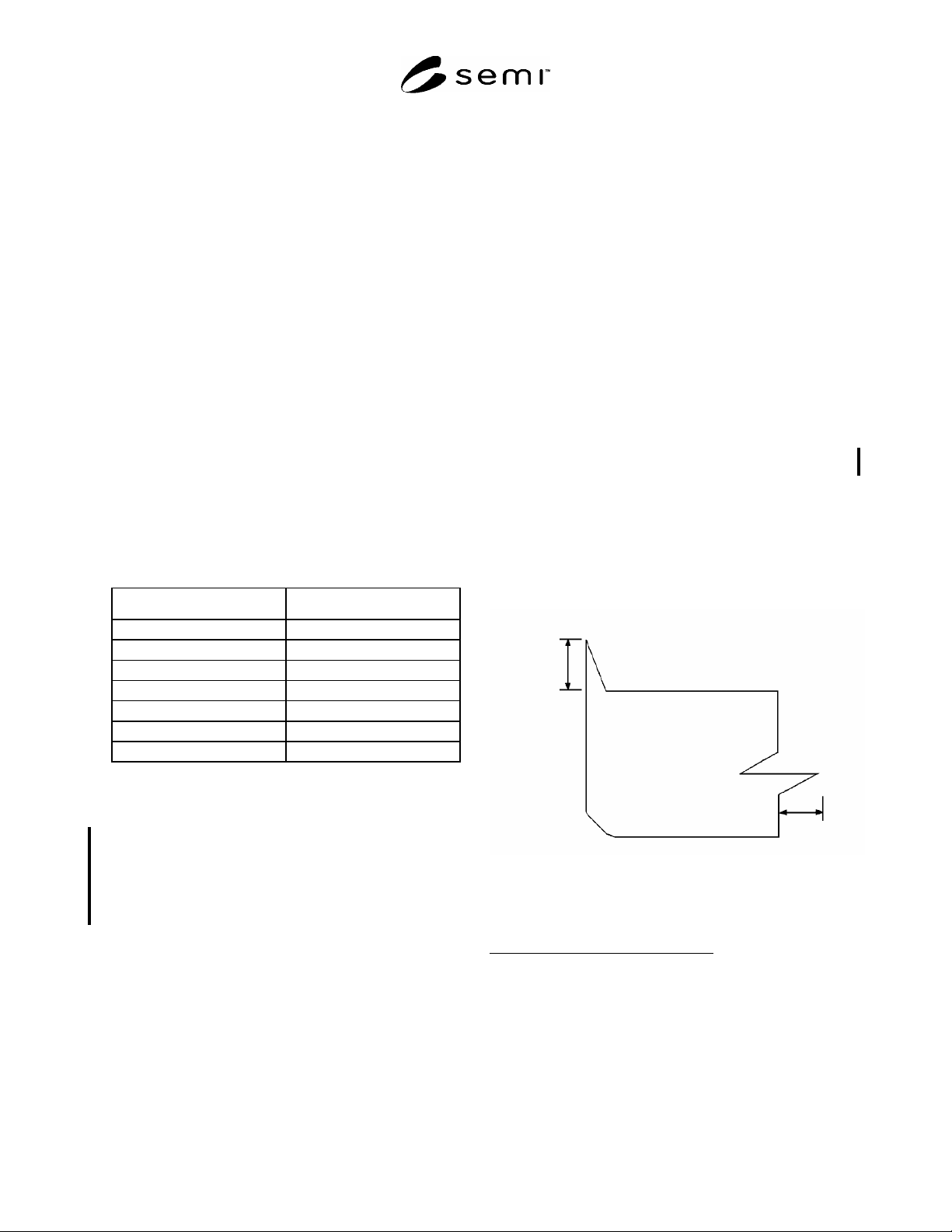
4.1.1 burr height — maximum height of burr above the
plane which it protrudes, (see Figure 1).
Figure 2
Burr Height
1 Electronic Industries Association of Japan, available through:
Japan Electronics and Information Technology Industries
Association, 3rd Fl., Mitsui Sumitomo Kaijo Bldg. Annex 11, Kanda
Surugadai 3-chome, Chiyoda-ku, Tokyo 101-0062, Japan,
http://www.jeita.or.jp/eiaj/english/
2 JEDEC Solid State Technology Association (aka the Joint Electron
Device Engineering Council), 2500 Wilson Boulevard, Arlington, VA
22201-3834, USA. Telephone: 703.907.7560; Fax: 703.907.7583,
Website: www.jedec.org
SEMI G70-0996 © SEMI 1996, 2004 2
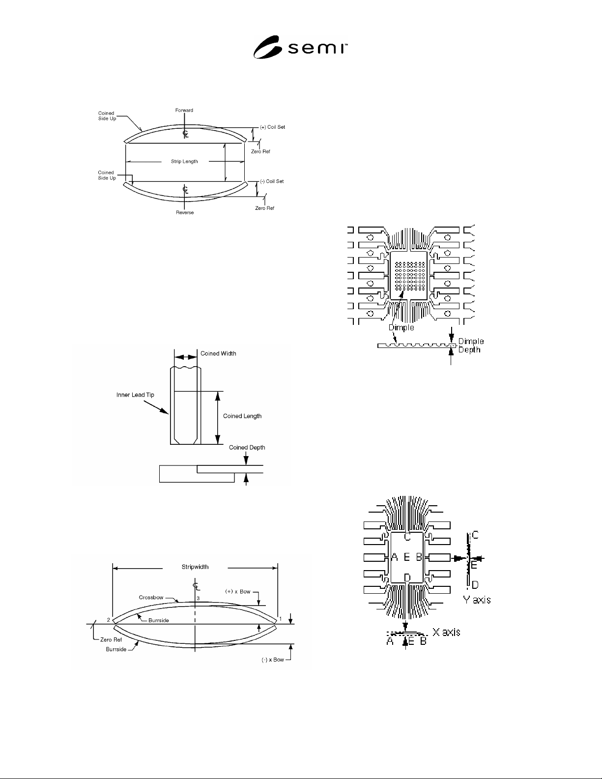
4.1.2 coil set — longitudinal bowing of the leadframe
strip length (see Figure 2).
Figure 2
Coil Set
4.1.3 coined depth — the difference in height between
the top surface of the coined area of an inner lead and
the top surface of the coined area at the tip of the lead.
Inner lead coining produces a flattened section of the
lead that is suitable for wire bonding (see Figure 3).
Figure 3
Coined Depth
4.1.4 crossbow — transverse bowing of the leadframe
(see Figure 4).
Figure 4
Crossbow
4.1.5 die pad dimple — a hollow formed in a die pad
using a half-etching technique or stamping to improve
the adhesive strength with the die or molding
compound and to reduce the stress between the die pad
and the die.
4.1.6 die pad dimple depth — the maximum depth of
the dimple (see Figure 5).
Figure 5
Die Pad Dimple Depth
4.1.7 die pad flatness — deviation of the center point
of die pad surface from a plane established by the four
corner points of die pad (see Figure 6).
Figure 6
Die Pad Flatness
3 SEMI G70-0996 © SEMI 1996, 2004
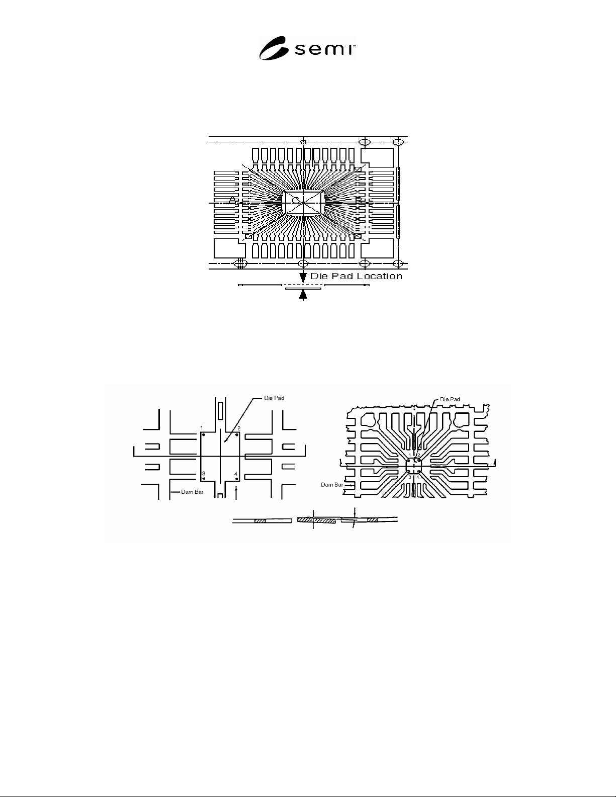
4.1.8 die pad location — deviation of the center point of die pad surface from a plane established by the dam bars
(see Figure 7).
Figure 7
Die Pad Location
4.1.9 die pad tilt — deviation of the plane of die pad from a condition parallel to the plane formed by the dam bars
(see Figure 8).
Figure 8
Die Pad Tilt
4.1.10 downset depth — (see Figure 9).