semi合集-English.pdf - 第3页
SEMI E1-0697 © SEMI 1979, 2003 1 SEMI E1-0697 (Reapproved 1102) E SPECIFICATION FOR 3 inch, 100 mm, 125 mm, AND 150 mm PLASTIC AND METAL WAFER CARRIERS This specification was technically approved b y the Global Physical …

SEMI INTERNATIONAL STANDARDS
EQUIPMENT AUTOMATION HARDWARE
Semiconductor Equipment and Materials International

SEMI E1-0697 © SEMI 1979, 2003 1
SEMI E1-0697 (Reapproved 1102)
E
SPECIFICATION FOR 3 inch, 100 mm, 125 mm, AND 150 mm PLASTIC
AND METAL WAFER CARRIERS
This specification was technically approved by the Global Physical Interfaces and Carriers Committee and is
the direct responsibility of the North American Physical Interfaces and Carriers Committee. Current edition
approved by the North American Physical Interfaces and Carriers Committee on July 21, 2002. Initially
available at www.semi.org October 2002; to be published November 2002. Orignally published in 1979;
previously published June 1997.
E The designation of SEMI E1 was updated during the 0303 publishing cycle to reflect the editorial
modification of SEMI E1.5 via PIP form.
1 Scope
1.1 This specification covers the dimensional
requirements for plastic and metal wafer carriers used
for the processing and handling of 3 inch, 100 mm, 125
mm, and 150 mm diameter wafers. The specification
has two classifications: General Usage and Auto
Transport Usage. General Usage is a basic guideline
that covers 3 inch, 100 mm, 125 mm, and 150 mm
wafer sizes. Auto Transport Usage is intended to meet
the in-use requirements for the interface of wafer
carriers with automated wafer processing equipment.
Auto Transport Usage covers the 125 mm and 150 mm
sizes.
1.2 To meet these specifications, carriers must be
manufactured within the dimensional limits and be
dimensionally stable within the specification when used
in accordance with manufacturers’ recommendations.
1.3 This standard does not purport to address safety
issues, if any, associated with its use. It is the
responsibility of the users of this standard to establish
appropriate safety health practices and determine the
applicability or regulatory limitations prior to use.
NOTE 1: Recommended usage should be agreed to between
user and supplier, since wafer carriers are manufactured from
a number of different materials by several manufacturing
methods.
2 Terminology
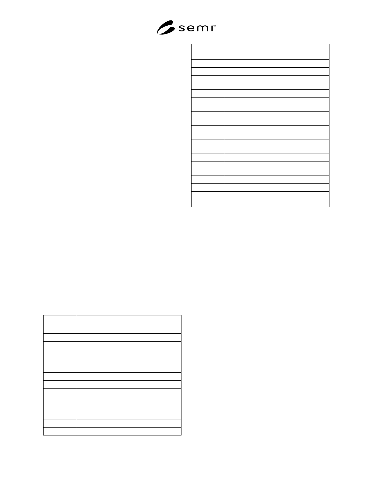
2.1 For a pictorial explanation of most of the selected
definitions, see Figure 1. Figure 1 symbols are defined
in Table 1.
2.2 Definitions
2.2.1 bar — (See “crossbar.”)
2.2.2 bar end — The end surface of the carrier that has
only one crossbar.
2.2.3 bar radius — The radius nearest the bar end of
the carrier on the crossbar. (See Figure 1, D5b, Type
II.)
2.2.4 bar web — The mass of material for structural
support which may or may not be present on the
crossbar. (See Figure 1, D5a, Type II.)
2.2.5 bar width — The distance or thickness of the bar
when measured perpendicular to the top face. (See
Figure 1, D5b.)
2.2.6 cassette — (See “wafer carrier.”)
2.2.7 crossbar — The mass of material connecting the
two sides of the carrier at the bar end of the carrier.
2.2.8 edge perimeter distance — The distance from the
edge of the wafer to the top face of the carrier. (See
Figure 1, D7.)
2.2.9 end wall — The wall of the carrier opposite the
bar end of the carrier.
2.2.10 flange — Mass of material on the exterior and
perpendicular to the side walls.
2.2.11 hole — The area for the pin on another carrier to
enter for transferring wafers. (See Figure 1, C8.)
2.2.12 lot — (See “hole.”)
2.2.13 parallelism tolerance — The minimum and
maximum dimension allowance for the opposite
pockets to vary in relation to their distance from the
crossbar end of the carrier. (See Figure 1, D1.)
2.2.14 pin — The mass of material which enters the
hole or slot of another carrier for transferring wafer.
(See Figure 1, C7.)
2.2.15 pin and hole center distance from pocket
centerline —The distance from centerline of either the
pin or hole to the closest pocket centerline. (See Figure
1, C9.)
2.2.16 pocket — The area in which the wafer is located
in the carrier.
2.2.17 pocket centerline — The imaginary line which
bisects each pocket.
SEMI E1-0697 © SEMI 1979, 2003 2
2.2.18 pocket depth — The distance from the pocket
flat to its own pocket nose, not to the opposite pocket.
(See Figure 1, C2.)
2.2.19 pocket flat — The width of the pocket along the
vertical walls at its narrowest distance. (See Figure 1,
C3.)
2.2.20 pocket nose — The top of the mass of material
between adjacent pockets.
2.2.21 pocket nose radius — The radius on the pocket
nose.
2.2.22 pocket size — The distance between opposite
pocket flats. (See Figure 1, C4.)
2.2.23 pocket spacing — The distance between pocket
centerlines. (See Figure 1, B2.)
2.2.24 pocket width — The width of the pocket at its
widest distance. (See Figure 1, C1.)
2.2.25 top face — The plane or surface of the carrier
from which side wafers enter into or out of the carrier.
2.2.26 track clearance — The unobstructed area
between the two carrier sides on the bar end. (See
Figure 1, D6; Figure 1a, D6a, D6b, D6c.)
2.2.27 wafer carrier — A device for the holding of
wafers for various processing steps in semiconductor
manufacturing.
2.2.28 wafer tilt — The possible unparallel position of
the wafer in relation to the bar end of the carrier when
the carrier is resting on the bar end. (Not shown in
Figure 1.)
2.2.29 wafer transfer — The act of relocating wafers
from one carrier into another. This can be accomplished
by several methods.
Table 1 Symbols Outline General Usage
Figure 1
Reference
Description
Overall Dimensions
A1 Length
A2 Width (with/without flange)
A3 Height (excluding pin)
Capacity
B1 Pockets per carrier
B2 Pocket spacing
B3 Center distance from the 1st to last pocket
Detail Dimensions
C1 Pocket width
C2 Pocket depth
C3 Pocket flat
C4 Pocket size
C5 Pin and hole location (width)
C6 Pin and hole location (length)
C7 Pin diameter and height
C8 Hole or slot
C9 Pin and hole center distance from pocket
center line
Machine Fit Specifications
D1 From the outside of the bar end to the
center line of the 1st pocket
D2 From the center line of the 1st pocket to the
closest point on the crossbar or web
D3 From the bar end of the carrier to the start
of the crossbar
D4 Center of the crossbar to the top face of the
carrier
D5 Crossbar specifications
D5a Bar web width on type II crossbar, or width
of the type III crossbar
D5b Bar width
D6 Track clearance
D7 Edge perimeter distance
Not shown — Wafer Tilt