semi合集-English.pdf - 第5000页
SEMI M13-1103 © SEMI 1988, 2003 12 NOTICE: SEMI makes no warranties or representatio ns as to the suitability of th e standards set forth herein for any particular application. Th e determination of the suitability of th…
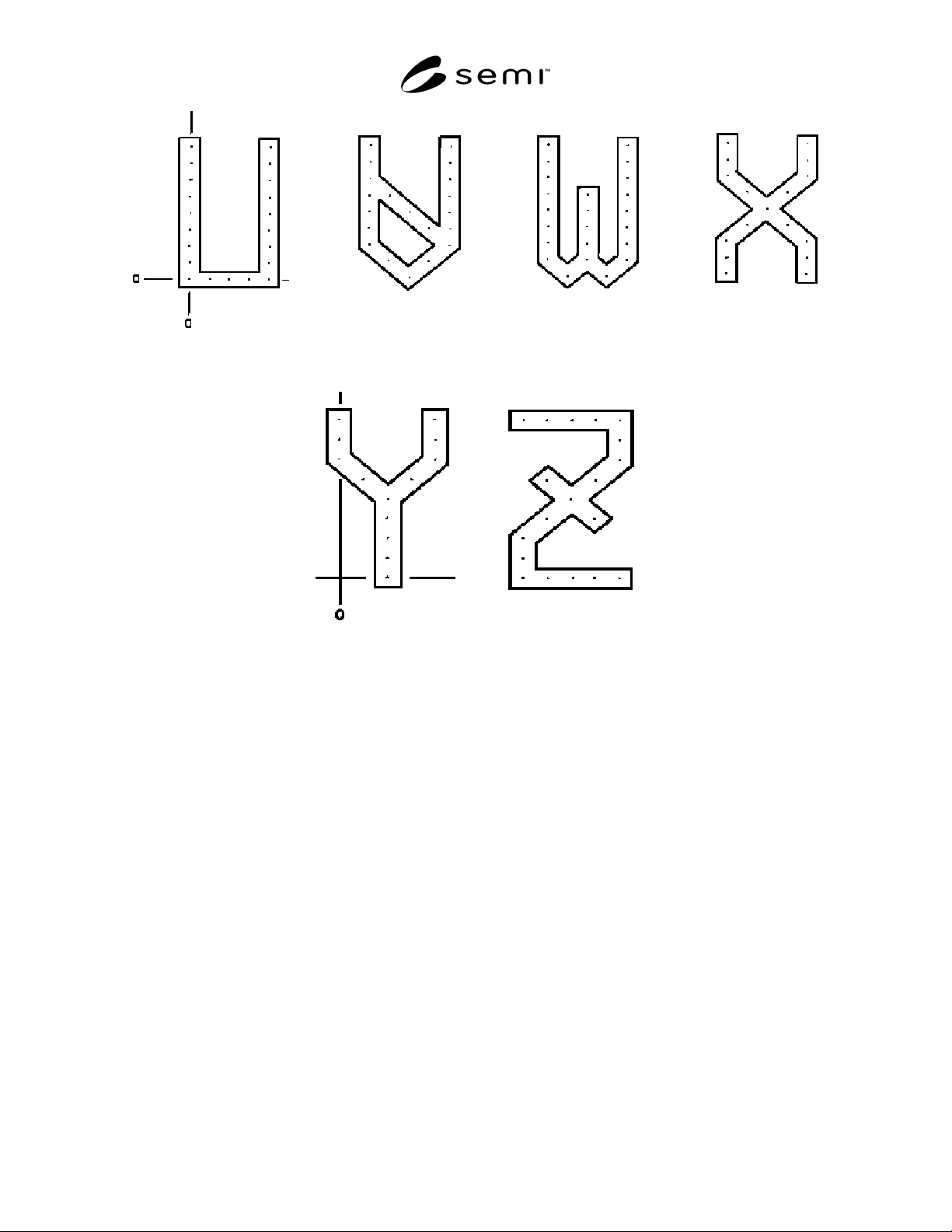
SEMI M13-1103 © SEMI 1988, 2003 11
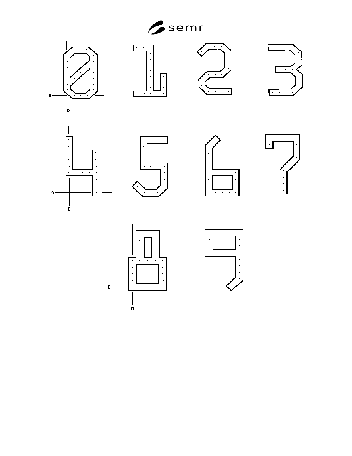
SEMI M13-1103 © SEMI 1988, 2003 12
NOTICE: SEMI makes no warranties or representations as to the suitability of the standards set forth herein for any
particular application. The determination of the suitability of the standard is solely the responsibility of the user.
Users are cautioned to refer to manufacturer' s instructions, product labels, product data sheets, and other relevant
literature, respecting any materials or equipment mentioned herein. These standards are subject to change without
notice.
By publication of this standard, Semiconductor Equipment and Materials International (SEMI) takes no position
respecting the validity of any patent rights or copyrights asserted in connection with any items mentioned in this
standard. Users of this standard are expressly advised that determination of any such patent rights or copyrights, and
the risk of infringement of such rights are entirely their own responsibility.

SEMI M13-1103 © SEMI 1988, 2003 13
RELATED INFORMATION 1
NOTICE: This related information is not an official part of SEMI M13 and is not intended to modify or supercede the official
standard. The standard should be referred to in all cases. SEMI makes no warranties or representations as to the suitability of the
material set forth herein for any particular application. The determination of the suitability of the material is solely the
responsibility of the user.
R1-1 Consideration for Reliable Automatic
Reading of the Marking
R1-1.1 The following suggestions are offered to assist
in assuring the most reliable automatic reading of the
alphanumeric marking.
R1-1.2 Character Stroke Thickness — If a 5 × 9 dot
matrix is chosen for marking, it is recommended that
the minimum dot size be 0.100 mm. With a higher
density dot matrix format, smaller dot diameters may be
employed. Stroke thickness should be constant within
20% over the entire character set so that the reader
settings may be optimized from the specific wafer run.
R1-1.3 Contrast — The character should have
sufficient contrast to be legible. Contrast may be
affected by depth and other conditions.
R1-1.4 Clear Zone — It is recommended that the area
immediately beneath, and a minimum of 0.500 mm
around, the marking characters be of uniform
reflectivity and free of any lithography and process
overlay edges.
NOTICE: SEMI makes no warranties or
representations as to the suitability of the standards set
forth herein for any particular application. The
determination of the suitability of the standard is solely
the responsibility of the user. Users are cautioned to
refer to manufacturer’s instructions, product labels,
product data sheets, and other relevant literature
respecting any materials mentioned herein. These
standards are subject to change without notice.
The user’s attention is called to the possibility that
compliance with this standard may require use of
copyrighted material or of an invention covered by
patent rights. By publication of this standard, SEMI
takes no position respecting the validity of any patent
rights or copyrights asserted in connection with any
item mentioned in this standard. Users of this standard
are expressly advised that determination of any such
patent rights or copyrights, and the risk of infringement
of such rights, are entirely their own responsibility.
Copyright by SEMI® (Semiconductor Equipment and Materials
International), 3081 Zanker Road, San Jose, CA 95134. Reproduction o
f
the contents in whole or in part is forbidden without express written
consent of SEMI.