semi合集-English.pdf - 第6145页
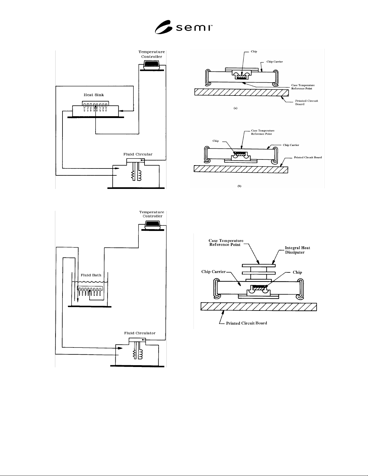
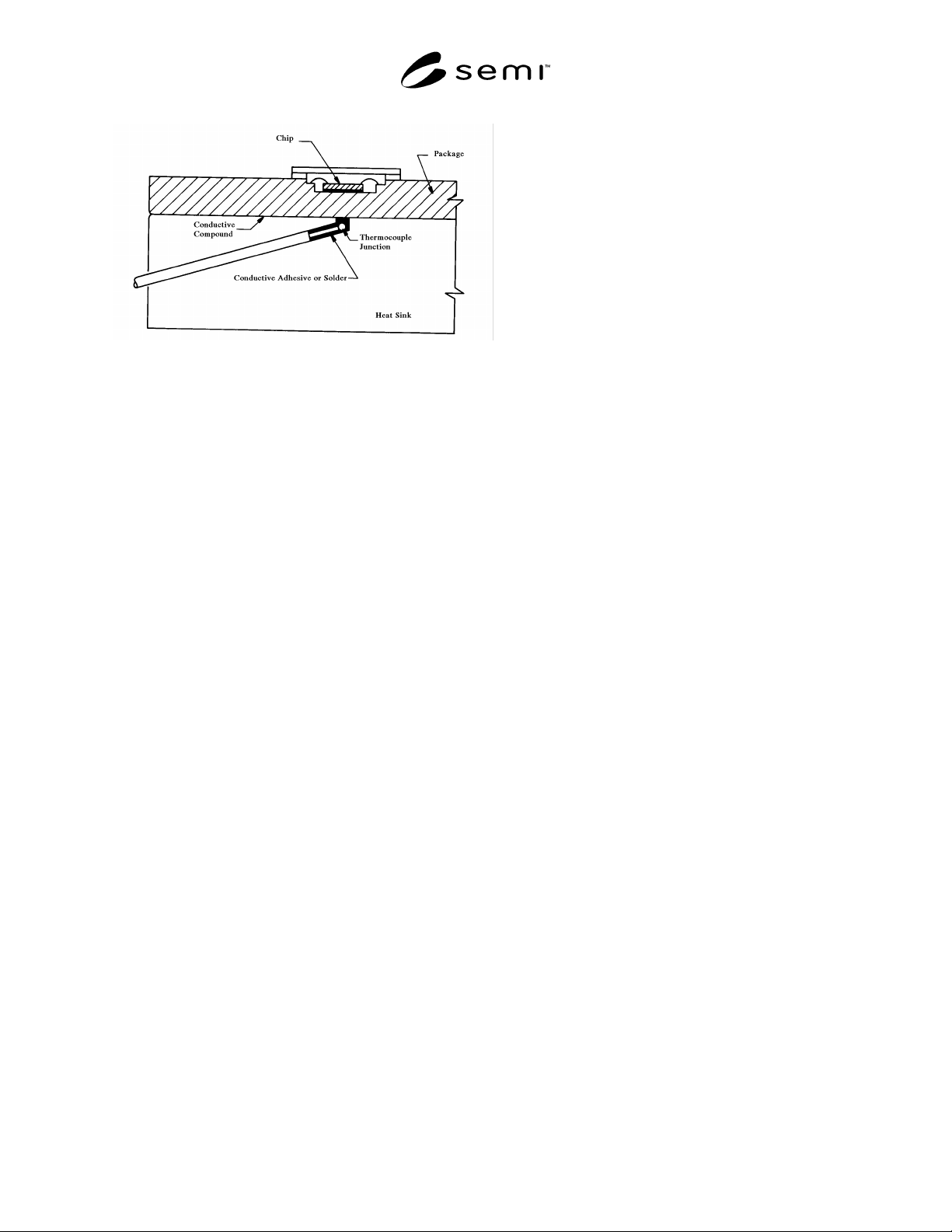
SEMI G30-88 © SEMI 198 6, 1988 5 Figure 1 Temperature-Controlled Heat Sink Assembly Figure 2 Temperature-Controlled Fluid Bath Assembly Figure 3 Reference Point Location for Case Tem perture Measurem ent of A) Cavity-Up …

SEMI G30-88 © SEMI 1986, 1988 4
measurement to be made is that of the temperature-
sensitive parameter, i.e., V
MC
, under operating
conditions with the measuring current, I
M
, used during
the calibration procedure. The microelectronic device
under test shall then be operated with heating power
(P
H
) applied. The temperature-sensitive parameter,
V
MH
, shall be measured with constant measuring
current, I
M
, that was applied during the calibration
procedure (See Step 1).
The heating power, P
H
, shall be chosen such that the
calculated junction-to-reference point temperature
difference as measured at V
MH
is greater than or equal
to 20°C. In accomplishing this, the device under test
should not be operated at such a high heating power
level that the on-chip temperature-sensing and heating
circuitry is no longer electrically isolated. Care should
also be taken not to exceed the design ratings of the
package-interconnect system, as this may lead to an
overestimation of the power being dissipated in the
active area of the chip due to excessive power losses in
the package leads and wire bonds. The values of V
MH
,
V
MC
, and P
H
are recorded during the power application
test.
The following data shall be recorded for these test
conditions:
a. Temperature-sensitive electrical parameters (V
F
,
V
EB
, or other appropriate TSP).
b. Junction temperature, T
J
, is calculated from the
equation:
T
J
= T
R
+ V
MH
− V
MC
()
∆V
MC
∆T
MC
ê
ê
ú
ú
−1
where T
R
= T
C
or T
M
c. Case or mounting surface temperature, T
C
or T
M
.
d. Power dissipation, P
H
.
e. Mounting arrangement (including package
mounting force).
3.3 Calculations of R
ΘJR
3.3.1 Calculations of Package Therm al Resistance —
The thermal resistance of a microelectronic device can
be calculated when the junction temperature, T
J
, has
been measured in accordance with procedures outlined
in Sections 3.1 and 3.2.
With the data recorded from each test, the thermal
resistance shall be determined from:
R
Θ
JR
=
T
J
−
T
R
P
H(package)
, junction - to reference point,
where R
QJR
=R
QJC
or R
QJM
and T
R
=T
C
or T
M
, respectively.
4 Summary Report
The following details shall be specified as appropriate:
a. Description of package, including thermal test chip,
location of case or chip carrier temperature
measurement(s), and heat sinking arrangement.
b. Test condition(s), as applicable (see Section 3).
c. Test voltage(s), current(s), and power dissipation of
test chip.
d. Recorded data for each test condition, as applicable.
e. Symbol(s) with subscript designation(s) of the
thermal characteristics determined.
f. Accept or reject criteria.
RELATED REFERENCES
1. Unencapsulated Thermal Test Chip, SEMI G32-86
Guideline, Book of SEMI Standards, Packaging
Volume.
2. Accepted Practices for Making Microelectronic
Device Thermal Characteristics Test — A User’s
Guide. JEDEC Engrg. Bull. No. 20, Jan. 1975
(Electronic Industries Assoc., Washington, D.C.).
3. Thermal Characteristics, Method 1012.1, MIL-STD-
883C Test Methods and Procedures for
Microelectronics, Nov. 4, 1980 (Rev. Aug. 15,
1984).
SEMI G30-88 © SEMI 1986, 19885
Figure 1
Temperature-Controlled Heat Sink Assembly
Figure 2
Temperature-Controlled Fluid Bath Assembly
Figure 3
Reference Point Location for Case Temperture
Measurement of A) Cavity-Up and B) Cavity—
Down Ceramic Packages
Figure 4
Reference Point Location for Case Temperature
Measurement of a Ceramic Package with an
Integral Head Dissipater
SEMI G30-88 © SEMI 1986, 1988 6
Figure 5
Mounting Surface Temperature Measurements
NOTICE: These standards do not purport to address
safety issues, if any, associated with their use. It is the
responsibility of the user of these standards to establish
appropriate safety and health practices and determine
the applicability of regulatory limitations prior to use.
SEMI makes no warranties or representations as to the
suitability of the standards set forth herein for any
particular application. The determination of the
suitability of the standard is solely the responsibility of
the user. Users are cautioned to refer to manufacturer’s
instructions, product labels, product data sheets, and
other relevant literature respecting any materials
mentioned herein. These standards are subject to
change without notice.
The user’s attention is called to the possibility that
compliance with this standard may require use of
copyrighted material or of an invention covered by
patent rights. By publication of this standard, SEMI
takes no position respecting the validity of any patent
rights or copyrights asserted in connection with any
item mentioned in this standard. Users of this standard
are expressly advised that determination of any such
patent rights or copyrights, and the risk of infringement
of such rights, are entirely their own responsibility.
Copyright by SEMI® (Semiconductor Equipment and Materials
International), 3081 Zanker Road, San Jose, CA 95134. Reproduction o
f
the contents in whole or in part is forbidden without express written
consent of SEMI.