semi合集-English.pdf - 第4959页
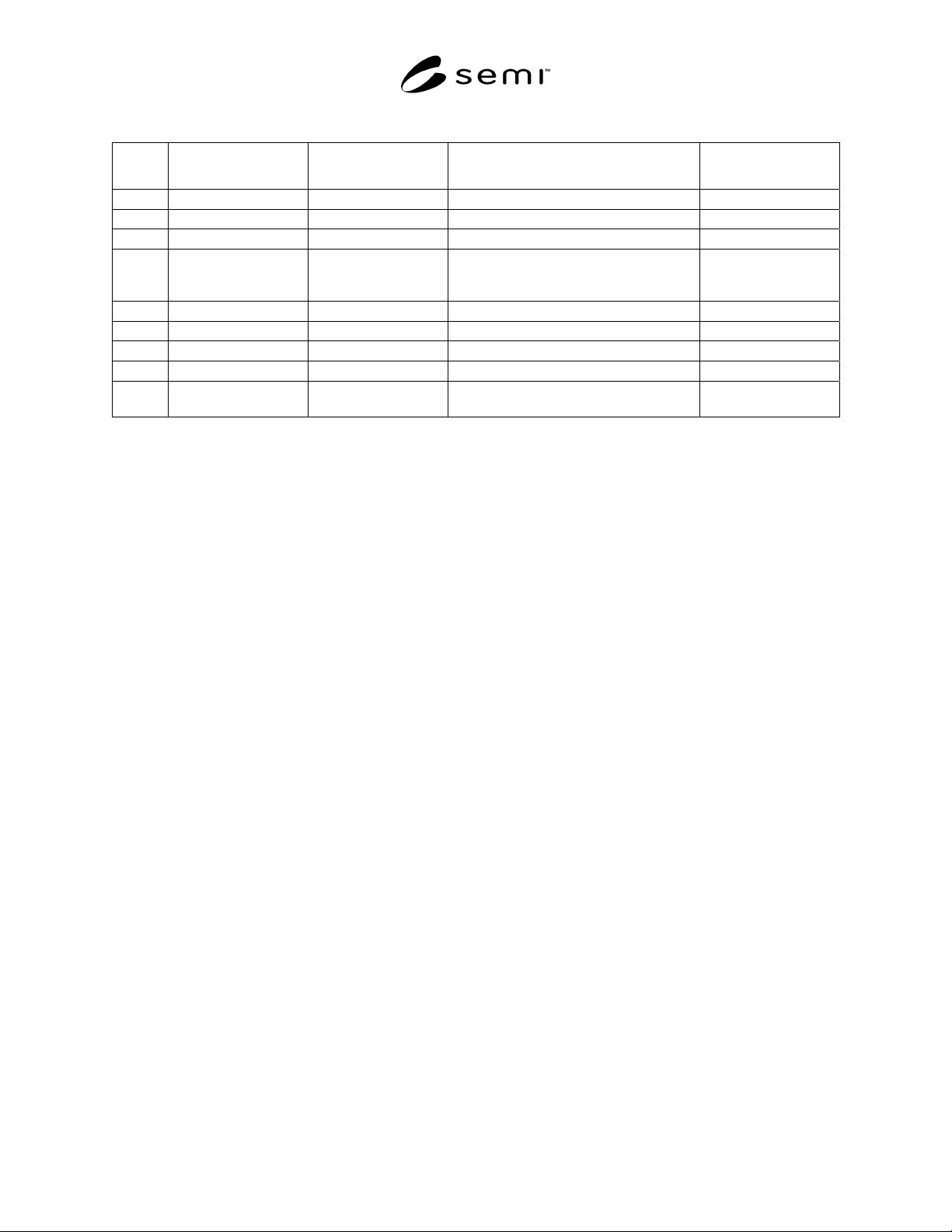
SEMI M11-0704 © SEMI 1988, 2004 16 Table 1 IC Epitaxial Wafers - Basic Surface Criter ia Item Characteristics Maximum Acceptability Limits Test Method Notes and Reference Documents 1 Stacking Faults 1 per cm 2 SEMI MF172…

SEMI M11-0704 © SEMI 1988, 2004 15
6 Requirements
6.1 As a minimum, the substrate shall conform to
SEMI M1 and the appropriate individual polished
monocrystalline silicon wafer standard.
6.2 Epitaxial wafer defects shall not exceed the limit as
given in Table 1.
6.2.1 Limits for slip, which may require destructive
testing, shall be specified in a purchase order together
with an appropriate test method. In the absence of
another specification, the wafer will contain no slip
lines within the quality area. (See Table 1, Note 1.)
NOTE 7: When an unetched wafer is observed for slip it is
impossible to differentiate between slip and linear misfit lines.
6.3 Layer Thickness Variation — Unless otherwise
specified, the thickness variation shall be determined
from value measured at the center and locations
centered 12 mm ± 1 mm from the periphery, on
diameters both parallel and perpendicular to the
primary flat,
100
tt
tt
(%)Variation
minmax
minmax
×
+
−
=
where t
max
and t
min
denote the maximum and minimum
thickness values measured. The 12 mm locations have
been defined based on instrument processing and
fixturing considerations.
6.4 Layer Net Carrier Density Variation — The net
carrier density variation shall be determined from
values measured at the center and locations with center
of the probe at 12 mm ± 1 mm from the periphery, on
diameters both parallel and perpendicular to the
primary flat,
100
NN
NN
(%)Variation
minmax
minmax
×
+
−
=
where N
max
and N
min
denote the maximum and
minimum values measured. The 12 mm locations have
been defined based on instrument processing and
fixturing considerations.
7 Test Methods and Measurements
7.1 Measurements shall be carried out in conformance
with the specified SEMI Test Methods. Where no
methods are specified or where choices are given, the
supplier and purchaser shall agree in advance on the
means for making the measurement.
7.2 Substrates — Determine in accordance with
methods specified in SEMI M1.
7.3 Epitaxial Layer
7.3.1 Thickness — Determine in accordance with
SEMI MF95 or SEMI MF110.
NOTE 8: In the case of thin layers and graded doping
transitions, SEMI MF95 and SEMI MF110 may not be
suitable. See the scopes of these test methods to determine
their limitations. In all cases, there is a possibility that various
types of infrared reflectance instrumentation may result in
different values of epitaxial layer thickness. Therefore, the
instrumentation used shall be agreed upon between supplier
and purchaser.
7.3.2 Net Carrier Density — Determine by method(s)
agreed upon between supplier and purchaser.
NOTE 9: SEMI MF1392 and SEMI MF1393 are methods for
measuring net carrier density using a mercury probe contact.
If resistivity is measured, as by SEMI MF374 or SEMI
MF525, conversion to dopant density shall be made using
SEMI MF723. Net carrier density of very heavily doped
layers (or substrates) may be found using SEMI MF398. Net
carrier density profiles may be determined directly in
accordance with SEMI MF1392 or SEMI MF1393 or
indirectly in accordance with SEMI MF672, with conversion
from resistivity to net carrier density in accordance with
SEMI MF723. If the method used for determining the net
carrier density profile is not the same as that used to
determine the center-point net carrier density, correlation
between the two methods used shall be established.
7.3.3 Epitaxial Wafer Defects — Determine in
accordance with the methods given in Table 1.
7.3.3.1 Surface inspection shall be performed before
any other testing. Wafers may be cleaned prior to
inspection to minimize difficulty in the visual
inspection of defects other than foreign matter.
7.3.3.2 Slip — Determine by methods agreed upon
between supplier and purchaser.
7.3.3.3 Automatic surface inspection technology is
being developed to detect and discriminate surface
defects. The extended definitions in Section 4.3 are
intended to facilitate this development.
NOTE 10: For observation of gross slip, examination of the
epitaxial layer under the illumination conditions specified in
Section 12.2 of SEMI MF523 may suffice. For more
demanding applications, it may be desirable to etch the
surface in accordance with SEMI MF1726 prior to the visual
inspection.
7.4 If substrates of different type and net carrier
density than the product substrates are to be used for
deposition control, their type, resistivity, and quantity
per run or lot shall be agreed upon between supplier and
purchaser.
SEMI M11-0704 © SEMI 1988, 2004 16
Table 1 IC Epitaxial Wafers - Basic Surface Criteria
Item Characteristics
Maximum
Acceptability Limits
Test Method
Notes and Reference
Documents
1 Stacking Faults 1 per cm
2
SEMI MF1726 1
2 Slip None SEMI MF523 or SEMI MF1726 1, 5, 6
3 Dislocations None SEMI MF1726 1
4 Total Localized
Light Scatterers
2000 per m
2
! 0.5 µm LSE, based on calibration of
surface scanning inspection systems with
latex spheres, 90% capture rate
1, 7
Table 2
5 Haze None SEMI MF523 Section 12.2 4, 7
6 Scratches None SEMI MF523 Section 12.2 2, 7
7 Edge Chips None SEMI MF523 Section 12.2
8 Foreign Matter None SEMI MF523 Section 12.3 4
9 Back Surface
Contamination
None SEMI MF523 Section 12.4 4
NOTE 1: Defect limits shall apply to quality area, which is defined as the entire wafer surface except a defined outer annulus of 4 mm and any
area included in a window where there is a laser identification mark.
NOTE 2: The cumulative AQL for both front surface and back surface of wafer is 2.5.
NOTE 3: The cumulative AQL for both front surface and back surface of wafer is 1.0.
NOTE 4: Any adherent contaminants, such as stains, glovemarks, dirt, smudges, warps, and solvent residues. This characteristic does not include
point defects. Any nonadherent contamination or particulate matter easily removed by industry-accepted cleaning techniques shall not constitute
foreign matter or haze.
NOTE 5: Test method(s) to be agreed upon between supplier and purchaser.
NOTE 6: For observation of gross slip, examine the epitaxial layer under illumination conditions specified in Section 12.2 of SEMI MF523. For
more demanding applications, it may be desirable to etch the surface in accordance with SEMI MF1726.
NOTE 7: In today’s technology, it may be possible to do this inspection using automated laser scanning systems; however, a standard test
procedure has yet to be developed. Application of automated inspection must be agreed upon between supplier and user.
8 Sampling
8.1 Unless otherwise specified, appropriate sample
sizes shall be selected from each lot according to
ANSI/ASQC Z1.4-1993. Quality characteristics shall
be assigned an acceptable quality level (AQL) in
accordance with ANSI/ASQC Z1.4-1993. Inspection
levels shall be agreed upon between supplier and
purchaser. Accept and reject criteria are to be based on
defective wafers, not on defective characteristics.
8.2 Unless otherwise specified, the following AQL’s
shall be assigned:
8.2.1 Epitaxial Layer Center-point Thickness and
Variation, 1%;
8.2.2 Epitaxial Layer Center Net Carrier Density and
Variation, 1%;
8.2.3 Epitaxial Wafer Defects, Cumulative, 2.5%.
9 Certification
9.1 Upon request of the purchaser in the contract or
order, a manufacturer’s or supplier’s certification that
the material was manufactured and tested in accordance
with this specification, together with a report of the test
results, shall be furnished at the time of shipment.
9.2 The supplier and purchaser may agree that the
material shall be certified as “capable of meeting”
certain requirements. In this context, “capable of
meeting” shall signify that the supplier is not required
to perform the appropriate tests in Section 7; however,
if the purchaser performs the test and the material fails
to meet the requirement, the material may be subject to
rejection.
10 Packing and Marking
10.1 Special packing requirements shall be subject to
agreement between the supplier and the purchaser.
Otherwise all wafers shall be handled, inspected, and
packed in such a manner as to avoid chipping,
scratches, and contamination, and in accordance with
the best industry practices to provide protection against
damage during shipment.
SEMI M11-0704 © SEMI 1988, 2004 17
10.2 The wafers supplied under this specification shall be identified by appropriately labeling the outside of each
box or container and each subdivision thereof in which it may reasonably be expected that the wafers will be stored
prior to further processing. Identification shall include supplier’s name and reference number, purchaser’s p.o.
number, quantity, dopant, orientation, conductivity type of substrates and epitaxial layers, carrier density, and
thickness of the epitaxial layer. The reference number assigned by the supplier shall provide ready access to
information concerning the fabrication history of the particular wafers in that lot. Such information shall be retained
on file at the manufacturer’s facility for at least one year after that particular lot has been shipped.
11 Guides
11.1 The specifications in the epitaxial guides are examples which were formed by a consensus of viewpoints. They
may or may not be used as a foundation to specify an epitaxial wafer for use in device manufacture. Their usefulness
can be increased by considering the guides prior to developing a device design or process. The required specification
is deter-mined by the device and the process design, the guides are suggestions from which a specification can
evolve.
11.2 An epitaxial guide can be viewed as a generic epitaxial wafer specification or as an example of a specification.
These tables provide common epitaxial wafer characteristics which describe starting wafers useful for the
manufacture of some twin tub CMOS devices.
11.3 The guides in Tables 3, 4, 5, 6, 7, 8, 9, and 10 provide a series of options intended to increase the awareness of
epitaxial specifications and to provide information from which a specification can be formulated.
11.4 SEMI M18 was used as a template for formulating these tables. When suitable to the application, the guides
can be used intact, reducing the proliferation of specifications and formats.
11.4.1 Table 3 is representative of 1.0 µm design rule epitaxial wafer criteria.
11.4.2 Table 4 is typical of an epitaxial wafer criteria for custom twin tub CMOS, 0.35 µm design rule devices, such
as, but not limited to ASIC’s, FPGA’s, linears, DSP’s, and microprocessors.
11.4.3 Table 5 is typical of an epitaxial wafer criteria for 0.35 µm design rule devices such as 64 megabit DRAM’s.
11.4.4 Table 6 is typical of epitaxial wafer criteria for twin tub CMOS, 0.25 µm design rule devices, such as, but
not limited to ASIC’s, FPGA’s, linears, DSP’s, and microprocessors.
11.4.5 Table 7 is typical of epitaxial wafer criteria for twin tub CMOS, 0.18 µm design rule devices.
11.4.6 Table 8 is typical of epitaxial wafer substrate criteria for a wafer pre-epitaxial that will be used in twin tub
CMOS, 0.25 µm design rule devices.
11.4.7 Table 9 is typical of epi wafer criteria for twin tub CMOS, 0.13 µm design rule devices.
11.4.8 Table 10 is typical of epi wafer criteria that can be used to develop a wafer specification for 90 nm Design
Rule CMOS devices.
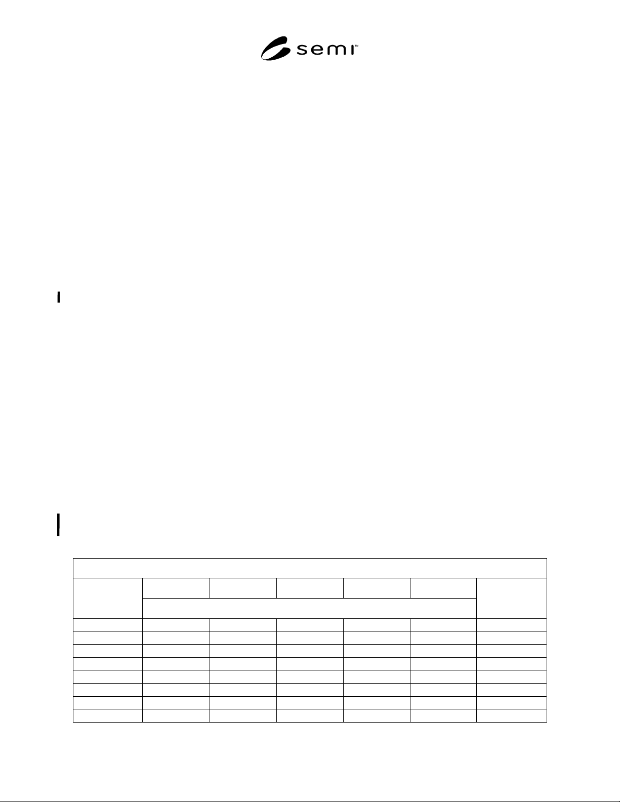
Table 2 Equivalent Units for Localized Light Scatterers
Diameter
1
100 125 150 200 300 Density
per m
2
Localized Light Scatterers per Wafer
Density
per cm
2
100 1 1 2 3 7 0.01
200 1 2 3 6 13 0.02
300 2 3 5 9 20 0.03
400 3 4 6 12 27 0.04
500 3 5 8 14 33 0.05
600 4 6 10 17 40 0.06
700 5 8 11 20 47 0.07
800 5 9 13 23 54 0.08