semi合集-English.pdf - 第5808页
SEMI P23-0200 © SEMI 1993 , 2000 31 Figure 26 Sensitivity Check Sheet – Wiring Pattern
SEMI P23-0200 © SEMI 1993, 2000 30
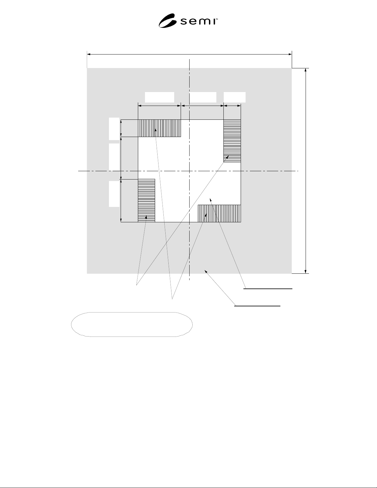
1250 um
1250 um
500 um1250 um
500 um1250 um
Film Pattern
Glass Pattern
(Vertical Line & Space Pattern)
1 : 1 Line & Space
(Horizontal Line & Space Pattern)
Line Width is Mask Design Rule Size.
Minimum 6000 um
Minimum 6000 um
Figure 25
Light Intensity Adjustment Pattern
SEMI P23-0200 © SEMI 1993, 200031
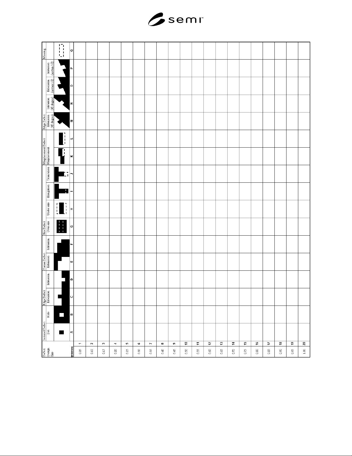
Figure 26
Sensitivity Check Sheet – Wiring Pattern
SEMI P23-0200 © SEMI 1993, 2000 32
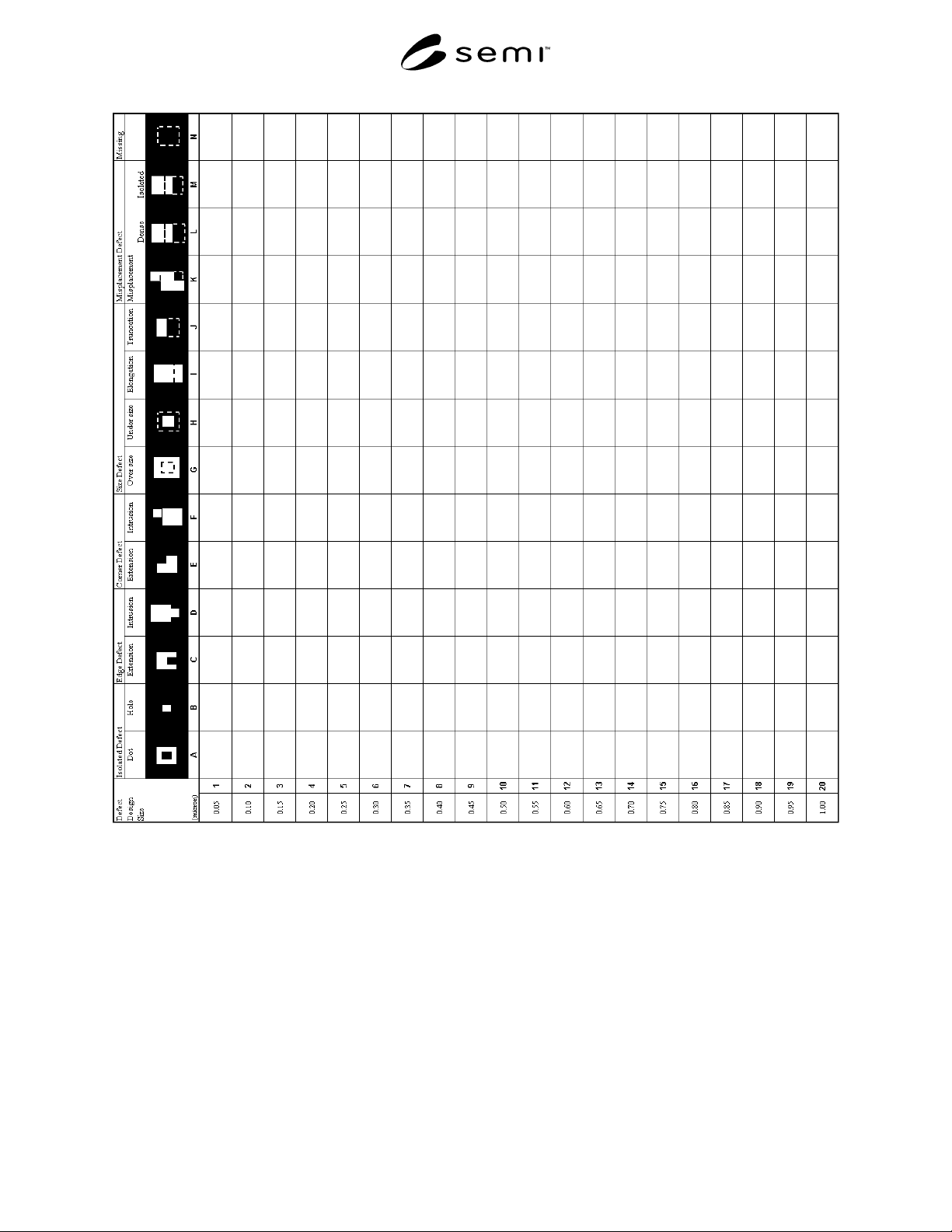
Figure 27
Sensitivity Check Sheet – Contact Hole Pattern
NOTICE: SEMI makes no warranties or representations as to the suitability of the guideline set forth herein for any
particular application. The determination of the suitability of the guideline is solely the responsibility of the user.
Users are cautioned to refer to manufacturer’s instructions, product labels, product data sheets, and other relevant
literature respecting any materials mentioned herein. These guidelines are subject to change without notice.
The user’s attention is called to the possibility that compliance with this guideline may require use of copyrighted
material or of an invention covered by patent rights. By publication of this guideline, SEMI takes no position
respecting the validity of any patent rights or copyrights asserted in connection with any item mentioned in this
guideline. Users of this guideline are expressly advised that determination of any such patent rights or copyrights,
and the risk of infringement of such rights, are entirely their own responsibility.
Copyright by SEMI® (Semiconductor Equipment and Materials
International), 3081 Zanker Road, San Jose, CA 95134. Reproduction o
f
the contents in whole or in part is forbidden without express written
consent of SEMI.