semi合集-English.pdf - 第7641页
SEMI T5-96 © SEMI 1996, 2004 4 7.5 In the standa rd specification, th e first character of the code line is located t oward the left side of t he code field. Figure 4 Code Field Locati on for Flatted Wafers Table 5 Loca …
SEMI T5-96 © SEMI 1996, 2004 3
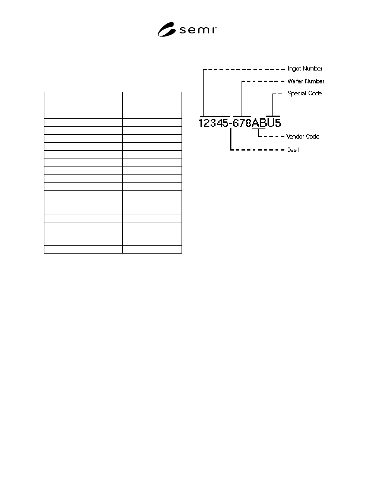
6.2 If the optional special code characters are used to
indicate doping, surface orientation, the symbols shown
in Table 4 will be employed.
Table 4 Special Code Characters
Parameter Code Definition
Device surface orientationand flat
location
V V - Groove
D Dovetail
Dopant U Undoped
C Carbon
R Chromium
T Tellurium
I Indium
S Silicon
L Sulfur
Z Zinc
E Selenium
Front Surface Orientation 0 100
A, B 111 A or B
2 100 (2°off)
3 100 (other off
orientation)
4 other orientation
5 other flats
6.3 An example of the code is given in Figure 3.
Figure 3
Example of Code for 3" Wafer
7 Code Field Location
7.1 Code field shall be located on the polished front
surface of wafers or on the polished or etched back
surface of wafers as shown in Table 5.
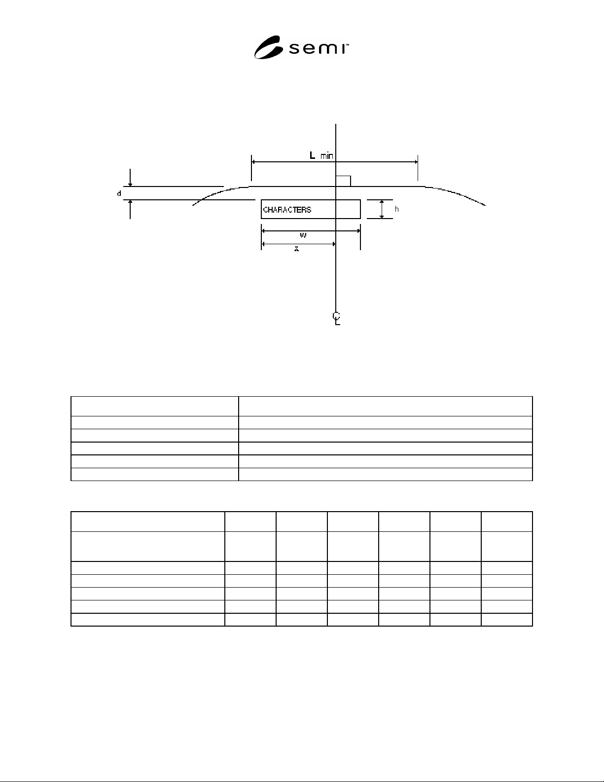
7.2 Code field is located as shown in Figure 4 and
Table 6.
7.3 All characters must be contained within the code
field along the major flat. The top of the characters is
toward the side of the code field nearest the flat, see
Figure 4.
7.4 Dimensions — See Figure 4 and Table 6.
SEMI T5-96 © SEMI 1996, 2004 4
7.5 In the standard specification, the first character of the code line is located toward the left side of the code field.
Figure 4
Code Field Location for Flatted Wafers
Table 5 Location of Code Field
Wafer Diameter Location of Code Field
2" Front (standard); Back surface (alternate)
3" Front (standard); Back surface (alternate)
100 mm Front surface
125 mm Front surface
150 mm Front surface
Table 6 Code Field Location and Dimensions
Parameter (mm) 2" 3" 3" 100 mm 125 mm 150 mm
Configuration Character Dimension(See
Tables 1 and 2)
B B A
#1
A A A
L min 14.23 19.05 19.05 30.0 40.0 55.0
x 7.1 9.5 9.5 15.0 20.0 27.5
w 14.0 14.0 19.0 27.0 27.0 27.0
d 1.0 1.0 1.0 1.0 1.0 1.0
h 1.4 1.4 2.4 2.4 2.4 2.4
#1: For 3" wafers, only 13 characters are allowed due to limitations on the size of the code field.
SEMI T5-96 © SEMI 1996, 2004 5
8 Character Alignment
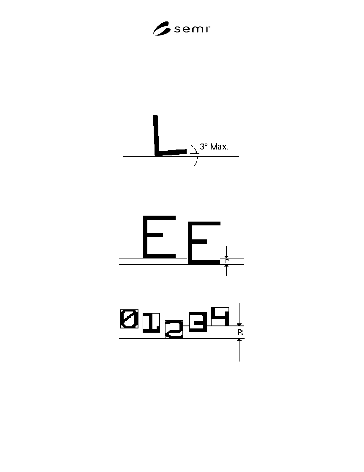
8.1 Character Skew — 3 degrees maximum allowable (see Figure 5).
8.2 Maximum character misalignment (see Figures 6 and 7).
8.2.1 Maximum adjacent character misalignment allowable is 0.230 mm.
8.2.2 Maximum line character misalignment allowable is 0.460 mm.
Figure 5
Character Skew
Figure 6
Adjacent Character Misalignment
Figure 7
Line Character Misalignment