semi合集-English.pdf - 第7632页
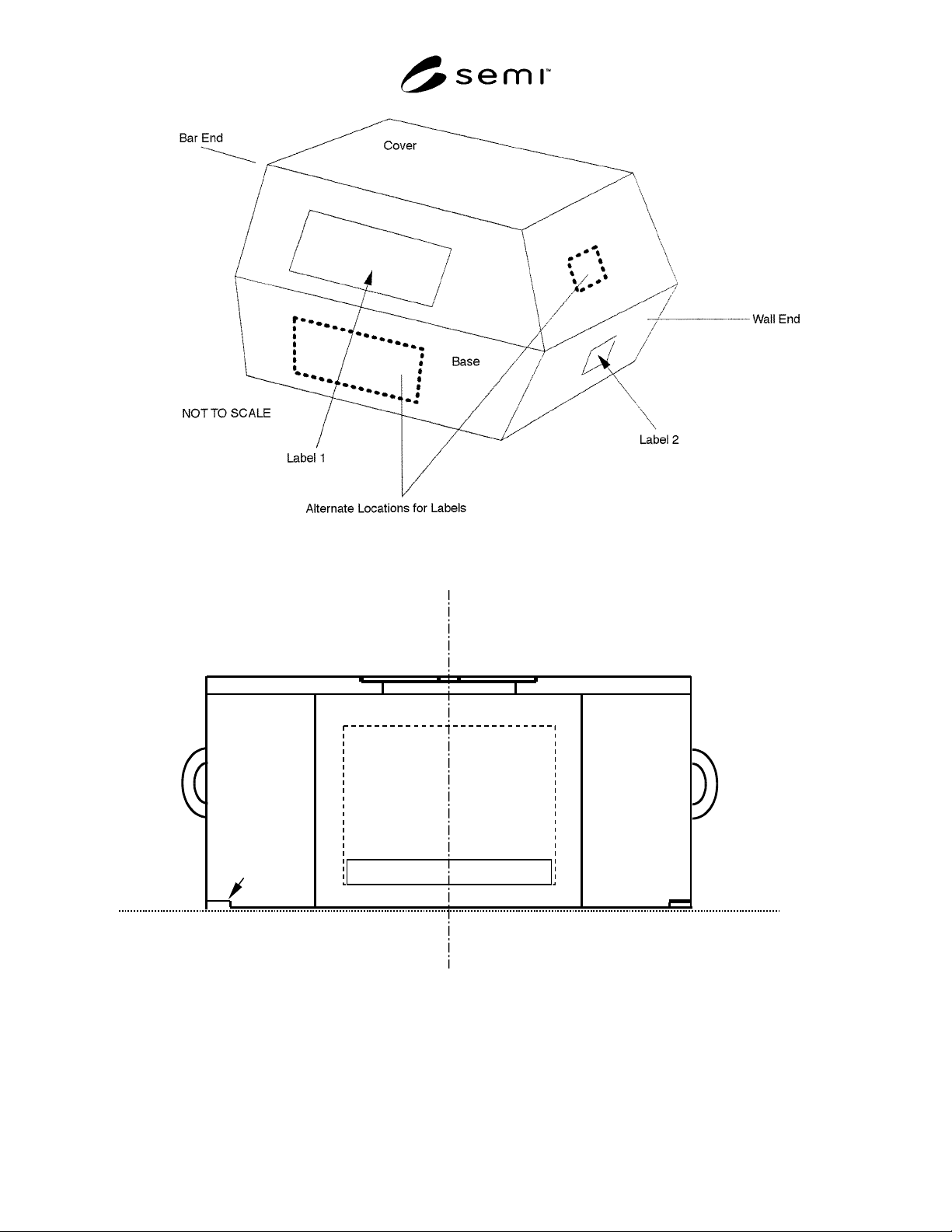
SEMI T3-0302 © SEMI 1995, 2002 14 Figure 7 Recomm ended and Alterna tiv e Locations for Labels on Wafer Boxes for Use with Wafers of 100 to 200 m m Diameter Bilateral Datum Plane Bottom Rail Human Handle ( o p tional ) H…
SEMI T3-0302 © SEMI 1995, 2002 13
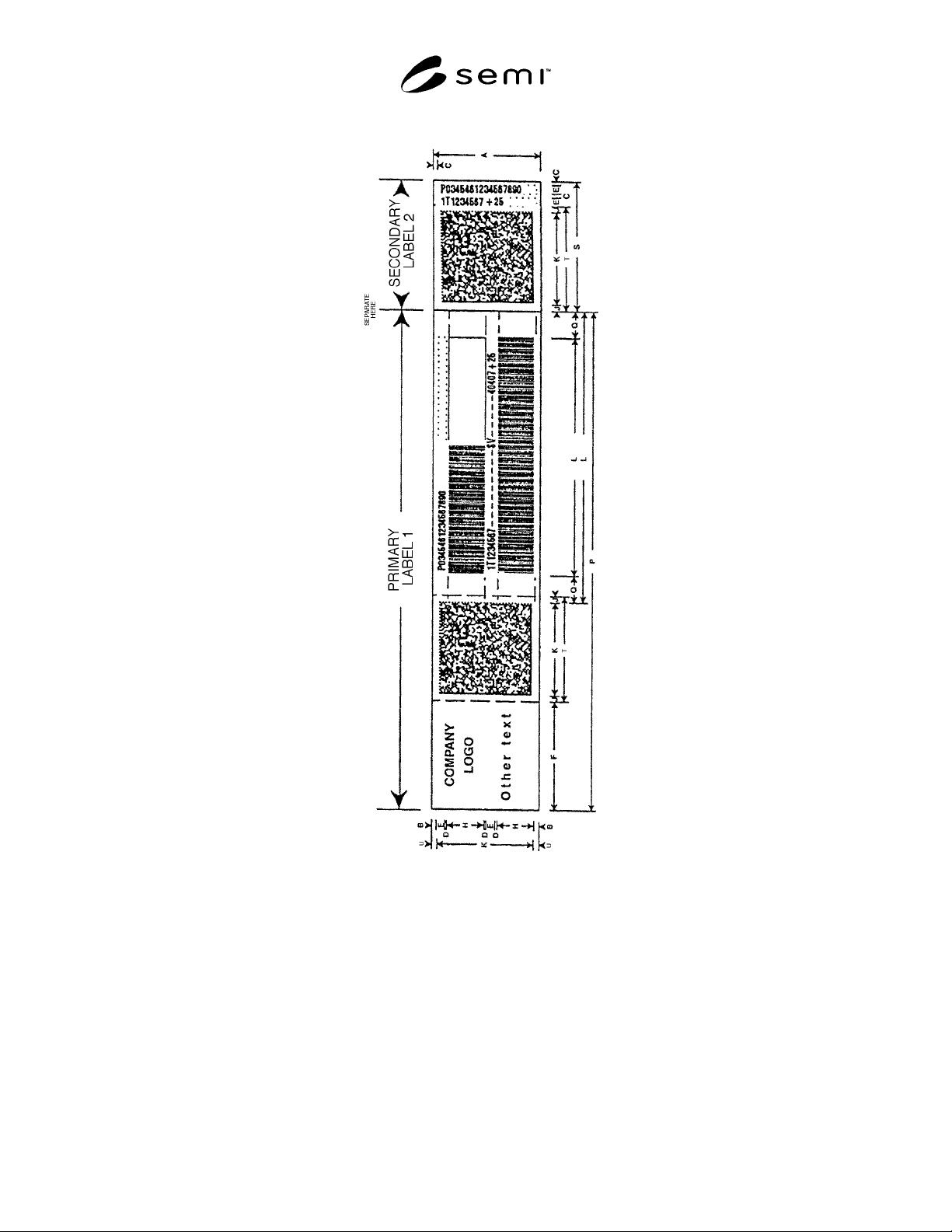
Figure 6
Labels with Bar Code, Human-Readable and Matrix Code Data Fields
SEMI T3-0302 © SEMI 1995, 2002 14
Figure 7
Recommended and Alternative Locations for Labels on Wafer Boxes for
Use with Wafers of 100 to 200 mm Diameter
Bilateral Datum Plane
Bottom Rail
Human Handle
(
o
p
tional
)
Horizontal Datum Plane of
Box Nest or Load Port
Rear Surface
Label Area
Preferred Label Location
Figure 8a
300 mm FOSB Rear Surface Label Locations
SEMI T3-0302 © SEMI 1995, 2002 15
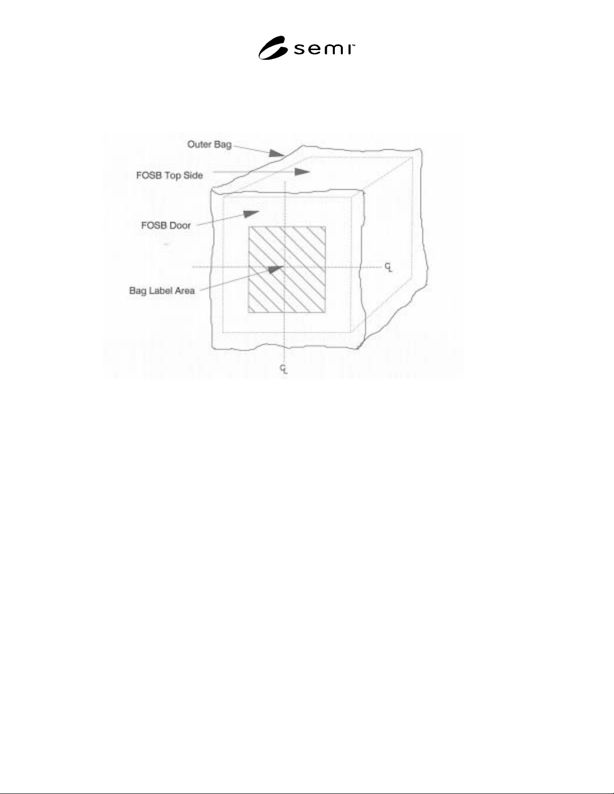
Figure 8b
FOSB Associated Outer Bag Label Location
NOTICE: SEMI makes no warranties or representations as to the suitability of the standards set forth herein for any
particular application. The determination of the suitability of the standard is solely the responsibility of the user.
Users are cautioned to refer to manufacturer' s instructions, product labels, product data sheets, and other relevant
literature, respecting any materials or equipment mentioned herein. These standards are subject to change without
notice.
By publication of this standard, Semiconductor Equipment and Materials International (SEMI) takes no position
respecting the validity of any patent rights or copyrights asserted in connection with any items mentioned in this
standard. Users of this standard are expressly advised that determination of any such patent rights or copyrights, and
the risk of infringement of such rights are entirely their own responsibility.