semi合集-English.pdf - 第4034页
SEMI F50-0200 © SEMI 2000 12 Table R2-1 Count of Events in Each Bin Time Bin i n Sec onds Magnit ude Bi n 0.0s < 0.2s 0.2s < 0.4s 0.4s < 0 .6s 0.6s < 0.8s >/= 0.8s > 80 − 90 % 11111 > 70 − 80 % 11111…

SEMI F50-0200 © SEMI 200011
RELATED INFORMATION 2
EXAMPLE OF MEASURED PERFORMANCE DATA REPORTED IN
MAGNITUDE AND DURATION BINS
NOTE: This related information is not an official part of
SEMI F50 and was derived from the work of the originating
task force. This related information was approved for
publication by full letter ballot procedures on December 15,
1999. Determination of the suitability of the material is solely
the responsibility of the user.
NOTE: This related information section is reprinted from
IEEE 1346. The IEEE disclaims any responsibility or liability
resulting from the placement and use in the described manner.
Information is reprinted with the permission of the IEEE.
R2-1 Excerpt from IEEE 1346 – Annex D
Constructing Coordination Charts
3
R2-1.1 The use of bins to count the number of voltage
sag events on a utility service is developed in IEEE
1346
4
as a step within a procedure for developing
number of sags per year contour graphs. The bin tables
are themselves useful as a tool for comparison of
voltage sag performance of electrical systems. The
paragraphs and tables below have been included to
explain the use of bins in the standardization of
historical or predicted events.
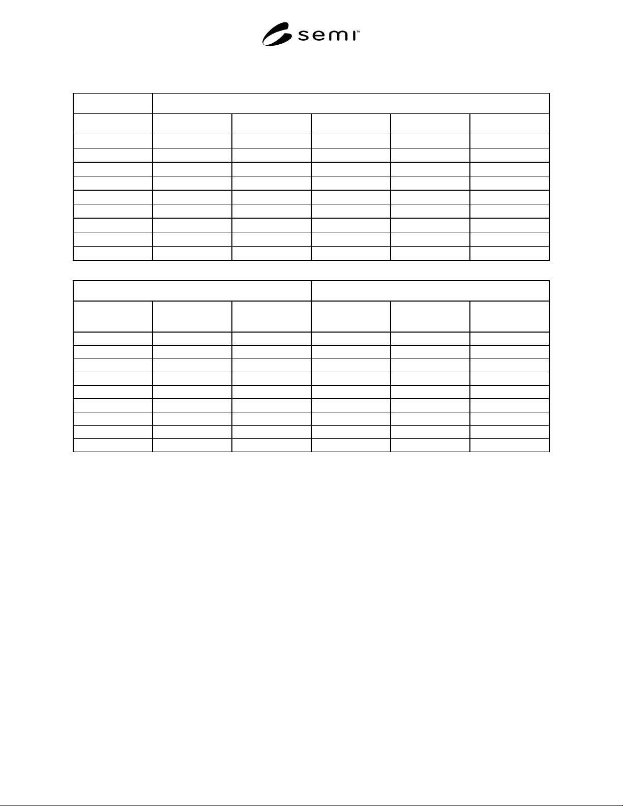
R2-1.2 Table R2-1 shows a grid of nine sag magnitude
ranges in rows and five sag duration ranges in columns.
The combination of nine rows and five columns
produce a total of 45 magnitude/duration bins. Each
measured or predicted sag will have a magnitude and
duration that fits in only one of the 45 bins. The
magnitude bin is a range of sag voltages expressed as a
percentage of nominal. The time bin is a range of sag
durations expressed as seconds. Each sag will have
associated with it one magnitude and one time bin. The
number in each table entry will correspond to the
number of sags that have magnitudes and times in the
same bins. Interruptions would go into the lower row
of bins according to the duration. The number bins
may vary depending on coordination needs for a
particular case. However, this selection of 45 bins is
reasonably convenient.
R2-1.3 For this example, assume each of the 45 bins
contains one sag event. This means there are 45 sags
per year and the characteristics of each sag fits in a
unique bin. The 15 bins in the lower-right corner have
3 Reprinted with the permission of The Institute of Electrical and
Electronic Engineers, Inc. (IEEE), 445 Hoes Lane, P.O. Box 1331
Piscataway, NJ 08855-1331, USA
4
IEEE 1346 — Recommended Practice for Evaluating Electrical
Power and System Compatibility with Electronic Process Equipment.
Copyright 1998 by The Institute of Electrical and Electronic
Engineers. All Rights Reserved.
bold italic highlighting to promote understanding as this
example continues.
R2-1.4 Table R1-2 shows the cumulative number of
sag events that are worse than or equal to each bin from
Table R1-1. “Worse than” means the magnitude is
lower and the duration is longer. The row and column
headings show only single values instead of ranges.
For example, there are 15 sags in the 50% magnitude,
0.4s entry of Table R1-2. The bold number 15 in Table
R1-2 is the sum of all 15 individual bold entries in
Table R1-1. This means 15 sags will have magnitude
less than or equal to 50% and duration longer than 0.4s.
SEMI F50-0200 © SEMI 2000 12
Table R2-1 Count of Events in Each Bin
Time Bin in Seconds
Magnitude Bin 0.0s < 0.2s 0.2s < 0.4s 0.4s < 0.6s 0.6s < 0.8s >/= 0.8s
> 80−90%
11111
> 70−80%
11111
> 60−70%
11111
> 50−60%
11111
> 40−50%
11
111
> 30−40%
11
111
> 20−30%
11
111
> 10−20%
11
111
0−10%
11
111
Table R2-2 Sum of Events Worse Than or Equal to Each Magnitude and Duration
Magnitude Time in Seconds
% of Nominal
Voltage
0.0s 0.2s 0.4s 0.6s 0.8s
90% 45 36 27 18 9
80% 40 32 24 16 8
70% 35 28 21 14 7
60% 30 24 18 12 6
50% 25 20
15
10 5
40% 20 16 12 8 4
30% 15 12 9 6 3
20%108642
10%54321
NOTICE: SEMI makes no warranties or representations as to the suitability of the guides set forth herein for any
particular application. The determination of the suitability of the guide is solely the responsibility of the user. Users
are cautioned to refer to manufacturer’s instructions, product labels, product data sheets, and other relevant literature
respecting any materials mentioned herein. These guides are subject to change without notice.
The user’s attention is called to the possibility that compliance with this guide may require use of copyrighted
material or of an invention covered by patent rights. By publication of this guide, SEMI takes no position respecting
the validity of any patent rights or copyrights asserted in connection with any item mentioned in this guide. Users of
this guide are expressly advised that determination of any such patent rights or copyrights, and the risk of
infringement of such rights, are entirely their own responsibility.
Copyright by SEMI® (Semiconductor Equipment and Materials
International), 3081 Zanker Road, San Jose, CA 95134. Reproduction o
f
the contents in whole or in part is forbidden without express written
consent of SEMI.

SEMI F51-0200 © SEMI 20001
SEMI F51-0200
GUIDE FOR ELASTOMETRIC SEALING TECHNOLOGY
This guide was technically approved by the Global Facilities Committee and is the direct responsibility of the
North American Facilities Committee. Current edition approved by the North American Regional Standards
Committee on December 15, 1999. Initially available on www.semi.org February 2000; to be published
February 2000.
1 Purpose
1.1 The purpose of this document is to introduce a
basic guide for the use of seals in semiconductor
fabrication equipment. Also, to introduce the diverse
chemical and physical requirements for the many
process applications, and to reduce cost of ownership
and improve up-time through the use of appropriate
sealing materials. It is important that equipment users,
suppliers, OEMs, and seal manufacturers use the same
terminology and that communication can take place at
the same level so that actual performance of the
equipment can be discussed.
2 Scope
2.1 This guide is applicable to the use of seals in
specific operating environments used in the fabrication
of semiconductor devices. The guide will aid in
defining the seal parameters for the various process
environments. It includes those elastomeric seals that
come in contact with process liquids and or gases.
2.2 This guide does not purport to address safety
issues, if any, associated with its use. It is the
responsibility of the users of this guide to establish
appropriate safety and health practices and determine
the applicability of regulatory limitations prior to use.
3 Limitations
3.1 The application of this guide is limited to
elastomeric sealing technology performance as used in
semiconductor manufacturing and related process
equipment.
4 Referenced Standards
4.1 SEMI Standards
SEMI C3 — Specifications for Gases
SEMI D9 — Definitions for Flat Panel Display
Substrates
SEMI E45 — Test Method for the Determination of
Inorganic Contamination from Minienvironments
SEMI F21 — Classification of Airborne Molecular
Contaminant Levels in Clean Environments
SEMI P5 — Specification for Pellicles
SEMI S4 — Safety Guideline for the
Segregation/Separation of Gas Cylinders Contained in
Cabinets
NOTE 1: As listed or revised, all documents cited shall be the
latest publications of adopted standards.
5 Terminology
5.1 Abbreviations and Acronyms
5.1.1 ATM — Atmospheric
5.1.2 BCD Bulk Chemical Dispensing System
5.1.3 CVD — Chemical Vapor Depo sition
5.1.4 DI — De-ionized
5.1.5 HDP — High Density Plasma
5.1.6 HF — Hydrofluoric Acid
5.1.7 LPCVD — Low Pressure Chemical Vapor
Deposition
5.1.8 MOCVD — Metal Organic Ch emical Vapor
Deposition
5.1.9 OEM — Original Equipment Manufacturer
5.1.10 PPB — Parts per Billion
5.1.11 PVD — Physical Vapor Deposition
5.1.12 RF — Radio Frequency
5.1.13 RTP — Rapid Thermal Process
5.1.14 T.O.C. (total organic carbons) hydrocarbons
which can appear in a process from a variety of sources
including breakdown of O-ring materials.
5.1.15 UPDI — Ultra Pure De-ionize d
5.1.16 UV — Ultraviolet
5.2 Definitions
5.2.1 acid
a corrosive material whose chemical
reaction characteristic is that of an electron acceptor
(SEMI F21, SEMI S4).
5.2.2 anion a negatively charged ion that is
attracted to an anode in electrolysis.