semi合集-English.pdf - 第6036页
SEMI G3-90 © SEMI 1 980, 199 6 8 35.56 ± 0.356 15.49 + 0.254 - 0.3 81 1 .93 - 2.39 7.75 ± 0.254 7.75 ± 0.254 mm 28VL SI 1.40 ± 0.014 0 .610 + 0.010 – 0. 015 0.076 – 0.094 0.340 ± 0.008 0.340 ± 0.008 in 35.56 ± 0.356 15.4…
SEMI G3-90 © SEMI 1980, 19967
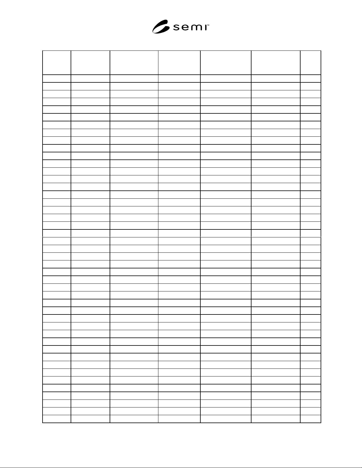
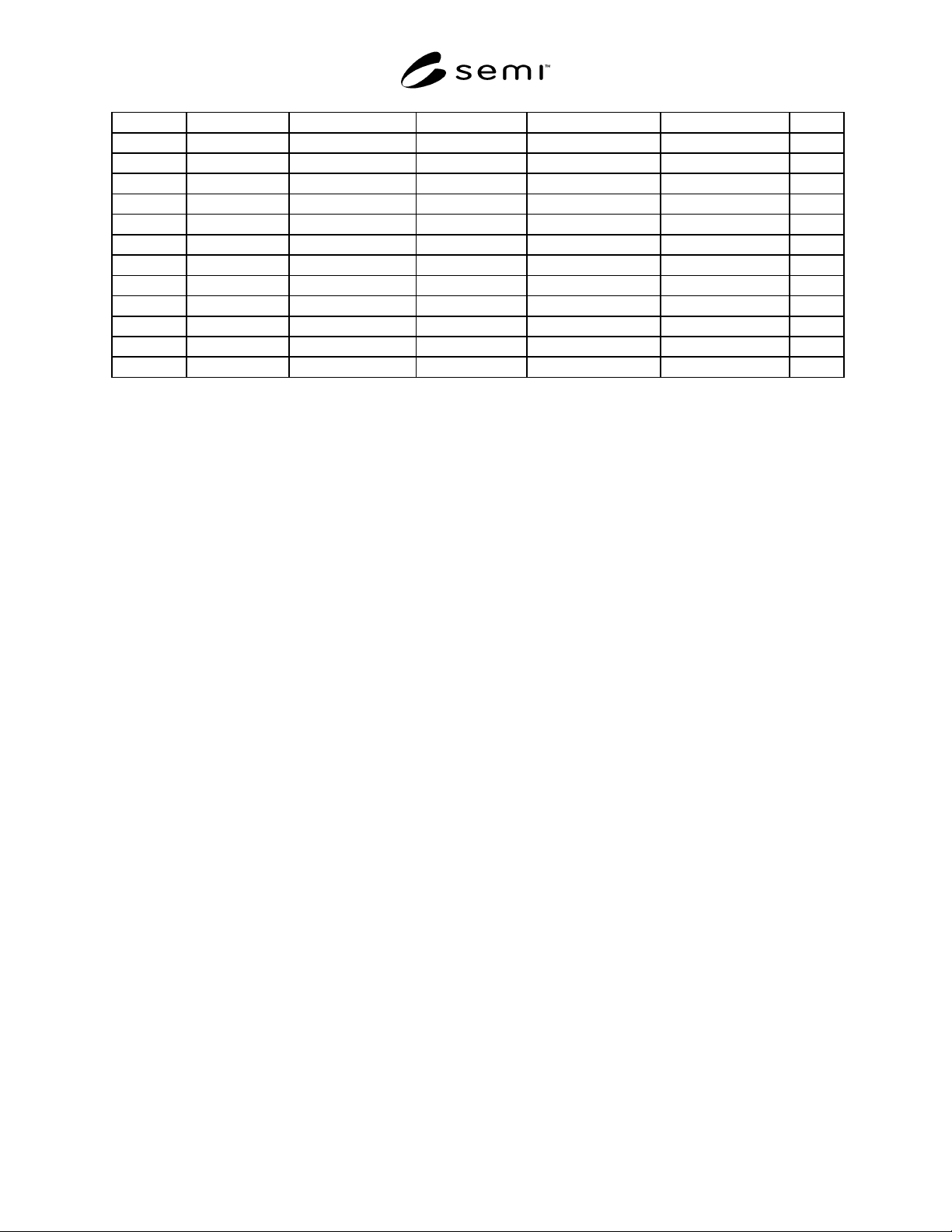
Table 1 Sidebrazed Laminate Packages Dimensions and Tolerance Requirements
Desription Package Length
Package Width
(Inc. Leadframe)
Package Thickness
Min. Max.
Cavity Length
(Measured at Cavity
Bottom)
Cavity Width
(Measured at Cavity
Bottom) Units
8MSI 0.520 ± 0.008 0.310 + 0.010 - 0.015 0.076 – 0.094 0.180 ± 0.005 0.150 ± 0.005 in
13.21 ± 0.203 7.87 + 0.254 - 0.381 1.93 – 2.39 4.57 ± 0.127 3.81 ± 0.127 mm
8LSI 0.520 ± 0.008 0.310 + 0.010 – 0.015 0.076 - 0.094 0.220 ± 0.005 0.175 ± 0.005 in
13.21 ± 0.203 7.87 + 0.254 - 0.381 1.93 - 2.39 5.59 ± 0.127 4.45 ± 0.127 mm
8VLSI 0.520 ± 0.008 0.310 + 0.010 – 0.015 0.076 - 0.094 0.260 ± 0.005 0.175 ± 0.005 in
13.21 ± 0.203 7.87 + 0.254 - 0.381 1.93 - 2.39 6.60 ± 0.127 4.45 ± 0.127 mm
14MSI 0.750 ± 0.010 0.310 + 0.010 – 0.015 0.076 – 0.094 0.180 ± 0.005 0.150 ± 0.005 in
19.05 ± 0.254 7.87 + 0.254 - 0.381 1.93 – 2.39 4.57 ± 0.127 3.81 ± 0.127 mm
14LSI 0.750 ± 0.010 0.310 + 0.010 – 0.015 0.076 - 0.094 0.220 ± 0.006 0.175 ± 0.005 in
19.05 ± 0.254 7.87 + 0.254 - 0.381 1.93 - 2.39 5.59 ± 0.152 4.45 ± 0.127 mm
14VLSI 0.750 ± .010 0.310 + 0.010 – 0.015 0.076 – 0.094 0.260 ± 0.006 0.175 ± 0.005 in
19.05 ± 0.254 7.87 + 0.254 - 0.381 1.93 – 2.39 6.60 ± 0.152 4.45 ± 0.127 mm
16MSI 0.800 ± 0.010 0.310 + 0.010 – 0.015 0.076 - 0.094 0.220 ± 0.006 0.175 ± 0.005 in
20.32 ± 0.254 7.87 + 0.254 - 0.381 1.93 - 2.39 5.59 ± 0.152 4.45 ± 0.127 mm
16LSI 0.800 ± 0.010 0.310 + 0.010 – 0.015 0.076 – 0.094 0.240 ± 0.006 0.175 ± 0.005 in
20.32 ± 0.254 7.87 + 0.254 - 0.381 1.93 – 2.39 6.10 ± 0.152 4.45 ± 0.127 mm
16VLSI 0.800 ± 0.010 0.310 + 0.010 – 0.015 0.076 - 0.094 0.320 ± 0.007 0.175 ± 0.005 in
20.32 ± 0.254 7.87 + 0.254 - 0.381 1.93 - 2.39 8.13 ± 0.178 4.45 ± 0.127 mm
18MSI 0.900 ± 0.010 0.310 + 0.010 – 0.015 0.076 – 0.094 0.220 ± 0.006 0.175 ± 0.005 in
22.86 ± 0.254 7.87 + 0.254 - 0.381 1.93 – 2.39 5.59 ± 0.152 4.45 ± 0.127 mm
18LSI 0.900 ± 0.010 0.310 + 0.010 – 0.015 0.076 - 0.094 0.265 ± 0.006 0.175 ± 0.005 in
22.86 ± 0.254 7.87 + 0.254 - 0.381 1.93 - 2.39 6.73 ± 0.152 4.45 ± 0.127 mm
18VLSI 0.900 ± 0.010 0.310 + 0.010 – 0.015 0.076 – 0.094 0.320 ± 0.007 0.175 ± 0.005 in
22.86 ± 0.254 7.87 + 0.254 - 0.381 1.93 – 2.39 8.13 ± 0.178 4.45 ± 0.127 mm
20MSI 1.000 ± 0.010 0.310 + 0.010 – 0.015 0.076 - 0.094 0.215 ± 0.005 0.175 ± 0.005 in
24.89 ± 0.254 7.87 + 0.254 - 0.381 1.93 - 2.39 5.46 ± 0.127 4.45 ± 0.127 mm
20LSI 1.000 ± 0.010 0.310 + 0.010 – 0.015 0.076 – 0.094 0.265 ± 0.006 0.175 ± 0.005 in
24.89 ± 0.254 7.87 + 0.254 - 0.381 1.93 – 2.39 6.73 ± 0.152 4.45 ± 0.127 mm
20VLSI 1.000 ± 0.010 0.310 + 0.010 – 0.015 0.076 - 0.094 0.320 ± 0.007 0.175 ± 0.005 in
24.89 ± 0.254 7.87 + 0.254 - 0.381 1.93 - 2.39 8.13 ± 0.178 4.45 ± 0.127 mm
22MSI 1.08 ± 0.011 0.410 + 0.010 – 0.015 0.076 – 0.094 0.250 ± 0.006 0.220 ± 0.006 in
27.34 ± 0.279 10.41 + 0.254 - 0.381 1.93 – 2.39 6.35 ± 0.152 5.59 ± 0.152 mm
22LSI 1.08 ± 0.011 0.410 + 0.010 – 0.015 0.076 - 0.094 0.285 ± 0.006 2.20 ± 0.006 in
27.34 ± 0.279 10.41 + 0.254 - 0.381 1.93 - 2.39 7.24 ± 0.152 5.59 ± 0.152 mm
22VLSI 1.08 ± 0.011 0.410 + 0.010 – 0.015 0.076 – 0.094 0.280 ± 0.006 0.260 ± 0.006 in
27.34 ± 0.279 10.41 + 0.254 - 0.381 1.93 - 2.39 7.11 ± 0.152 6.60 ± 0.152 mm
24MSI 1.20 ± 0.012 0.610 + 0.010 – 0.015 0.076 - 0.094 0.250 ± 0.006 0.250 ± 0.006 in
30.48 ± 0.305 15.49 + 0.254 - 0.381 1.93 - 2.39 6.35 ± 0.152 6.35 ± 0.152 mm
24LSI 1.20 ± 0.012 0.610 + 0.010 – 0.015 0.076 – 0.094 0.305 ± 0.010 0.305 ± 0.010 in
30.48 ± 0.305 15.49 + 0.254 - 0.381 1.93 – 2.39 7.75 ± 0.254 7.75 ± 0.254 mm
24VLSI 1.20 ± 0.012 0.610 + 0.010 – 0.015 0.076 - 0.094 0.340 ± 0.008 0.340 ± 0.008 in
30.48 ± 0.305 15.49 + 0.254 - 0.381 1.93 - 2.39 8.64 ± 0.203 8.64 ± 0.203 mm
28MSI 1.40 ± 0.014 0.610 + 0.010 – 0.015 0.076 – 0.094 0.250 ± 0.006 0.250 ± 0.006 in
35.56 ± 0.356 15.49 + 0.254 - 0.381 1.93 – 2.39 6.35 ± 0.152 6.35 ± 0.152 mm
28LSI 1.40 ± 0.014 0.610 + 0.010 – 0.015 0.076 - 0.094 0.305 ± 0.010 0.305 ± 0.010 in
SEMI G3-90 © SEMI 1980, 1996 8
35.56 ± 0.356 15.49 + 0.254 - 0.381 1.93 - 2.39 7.75 ± 0.254 7.75 ± 0.254 mm
28VLSI 1.40 ± 0.014 0.610 + 0.010 – 0.015 0.076 – 0.094 0.340 ± 0.008 0.340 ± 0.008 in
35.56 ± 0.356 15.49 + 0.254 - 0.381 1.93 – 2.39 8.64 ± 0.203 8.64 ± 0.203 mm
40MSI 2.00 ± 0.020 0.610 + 0.010 – 0.015 0.076 - 0.094 0.250 ± 0.006 0.250 ± 0.006 in
50.8 ± 0.508 15.49 + 0.254 - 0.381 1.93 - 2.39 6.35 ± 0.152 6.35 ± 0.152 mm
40LSI 2.00 ± 0.020 0.610 + 0.010 – 0.015 0.076 – 0.094 0.305 ± 0.010 0.305 ± 0.010 in
50.8 ± 0.508 15.49 + 0.254 - 0.381 1.93 – 2.39 7.75 ± 0.254 7.75 ± 0.254 mm
40VLSI 2.00 ± 0.020 0.610 + 0.010 – 0.015 0.076 - 0.094 0.340 ± 0.008 0.340 ± 0.008 in
50.8 ± 0.508 15.49 + 0.254 - 0.381 1.93 - 2.39 8.64 ± 0.203 8.64 ± 0.203 mm
48LSI 2.40 ± 0.025 0.610 + 0.010 – 0.015 0.076 – 0.094 0.305 ± 0.010 0.305 ± 0.010 in
60.96 ± 0.635 15.49 + 0.254 – 0.381 1.93 – 2.39 7.75 ± 0.254 7.75 ± 0.254 mm
48VLSI 2.40 ± 0.025 0.610 + 0.010 - 0.015 0.076 - 0.094 0.340 ± 0.008 0.340 ± 0.008 in
60.96 ± 0.635 15.49 + 0.254 – 0.381 1.93 - 2.39 8.64 ± 0.203 8.64 ± 0.203 mm
NOTICE: These standards do not purport to address safety issues, if any, associated with their use. It is the
responsibility of the user of these standards to establish appropriate safety and health practices and determine the
applicability of regulatory limitations prior to use. SEMI makes no warranties or representations as to the suitability
of the standards set forth herein for any particular application. The determination of the suitability of the standard is
solely the responsibility of the user. Users are cautioned to refer to manufacturer’s instructions, product labels,
product data sheets, and other relevant literature respecting any materials mentioned herein. These standards are
subject to change without notice.
The user’s attention is called to the possibility that compliance with this standard may require use of copyrighted
material or of an invention covered by patent rights. By publication of this standard, SEMI takes no position
respecting the validity of any patent rights or copyrights asserted in connection with any item mentioned in this
standard. Users of this standard are expressly advised that determination of any such patent rights or copyrights, and
the risk of infringement of such rights, are entirely their own responsibility.
Copyright by SEMI® (Semiconductor Equipment and Materials
International), 3081 Zanker Road, San Jose, CA 95134. Reproduction o
f
the contents in whole or in part is forbidden without express written
consent of SEMI.

SEMI G4-0302 © SEMI 1982, 2002 1
SEMI G4-0302
SPECIFICATION FOR INTEGRATED CIRCUIT LEADFRAME
MATERIALS USED IN THE PRODUCTION OF STAMPED
LEADFRAMES
This specification was technically approved by the Gobal Assembly and Packaging Committtee and is the
direct responsibility of the Japanese Assembly and Packaging Committee. Current edition approved by the
Japanese Regional Standards Committtee on November 26, 2001. Initially available at www.semi.org
December 2001; to be published March 2002. Originally published in 1994.
1 Scope
1.1 This specification covers the special requirements
for a metal strip to be used to fabricate integrated circuit
leadframes by stamping.
2 Applicable Documents
Regional standards such as ANSI/ASTM,CEN, EN
ISO, JIS, and MIL.
2.1 ANSI
1
/ASTMStandard
2
ASTM B 193 — Test Method for Resistivity of
Electrical Conductor Materials
ASTM B 601 — Standard Practice for Temper
Designations for Copper and Copper Alloys —
Wrought and Cast
ASTM E 8 — Standard Test Methods of Tension
Testing of Metallic Materials
ASTM E 228 — Standard Test Method for Linear
Thermal Expansion of Solid Materials with a Vitreous
Silica Delatometer
ASTM E 290 — Test Method for Semi-Guided Bend
Test for Ductility of Metallic Materials
ASTM E 384 — Test Method for Microhardness of
Materials
ASTM E 527 — Practice for Numbering Metals and
Alloys (UNS)
2.2 CES Standard
CES M0002-5 — Method of W-Bend Test for Metallic
Materials
2.3 EN Standard
EN 10 002 Part 1 — Metallic Materials, Tensile
Testing, Part 1: Method of Testing (at ambient
temperature)
1 ANSI, 1430 Broadway, New York, NY 10018
2 American Society for Testing and Materials, 100 Barr Harbor
Drive, West Conshohoken, PA 19428-2959
EN 133/10 — Copper and Copper Alloys: Plate, Sheet,
Strip, and Circles for General Purposes
EN 133/12 — Copper and Copper Alloys: Plate, Sheet,
and Circles for Boilers, Pressure Vessels, and Hot
Water Storage Units
2.4 ISO Standard
3
ISO 197-3 — Copper and Copper Alloys, Terms, and
Definitions, Part 3: Wrought Products
ISO 1190 Part 1 — Copper and Copper Alloys, Code of
Designation, Part 1: Designation of Materials
ISO 4287 Part 1 — Surface Roughness, Terminology,
Part 1: Surface and Its Parameters Trilingual Edition
ISO 6507 Part 1 — Metallic Materials, Hardness Test,
Vickers Test, Part 1: HV 5 to HV 100
ISO 6507 Part 2 — Metallic Materials, Hardness Test,
Vickers Test, Part 2: HV 0.2 to less than HV 5.
ISO 7438 — Metallic Materials, Bend Test
2.5 JIS Standard
4
JIS B0601 — Definitions and Designation of Surface
Roughness
JIS H0505 — Measuring Methods for Electrical
Resistivity and Conductivity of Non-Ferrous Materials
JIS H3100 — Copper and Copper Alloy: Plates, Sheets,
Strips
JIS H3110 — Phosphor Bronze and Nickel Silver:
Plates, Sheets, Strips
JIS Z2201 — Test Pieces for Tensile Test for Metallic
Materials
JIS Z2241 — Method of Tensile Test for Metallic
Materials
JIS Z2244 — Method of Vickers Hardness Test
3 ISO, 1 rue de Varembe, Case postale 56, CH01211 Geneva 20,
Switzerland
4 JIS, 4-1-24 Akasaka Minato-ku Tokyo, Japan