semi合集-English.pdf - 第6532页
SEMI G81-0703 © SEMI 2000, 2003 7 APPENDIX 1 WAFER MAP NOTICE : The material in this appendix is an official part of SEMI G81 and was approved by full letter ballot procedures on August 27, 2001. A1-1 This appendix shows…

SEMI G81-0703 © SEMI 2000, 2003 6
ReferenceDeviceX="4"
ReferenceDeviceY="-5"
RefDevicePosX="2"
RefDevicePosY="2"
/>
<Bin
BinCode="02"
BinQuality="Pass"
BinDescription="500MHz"
/>
<Data MapName="SortGrade" Version="1">
<Row><![CDATA[FFFF020CFFFF]]></Row>
<Row><![CDATA[FF14020C02FF]]></Row>
<Row><![CDATA[0202020C0116]]></Row>
<Row><![CDATA[0201140C0202]]></Row>
<Row><![CDATA[FF14020C02FF]]></Row>
<Row><![CDATA[FFFF020CFFFF]]></Row>
</Data>
</Device>
</Map>
SEMI G81-0703 © SEMI 2000, 2003 7
APPENDIX 1
WAFER MAP
NOTICE: The material in this appendix is an official part of SEMI G81 and was approved by full letter ballot
procedures on August 27, 2001.
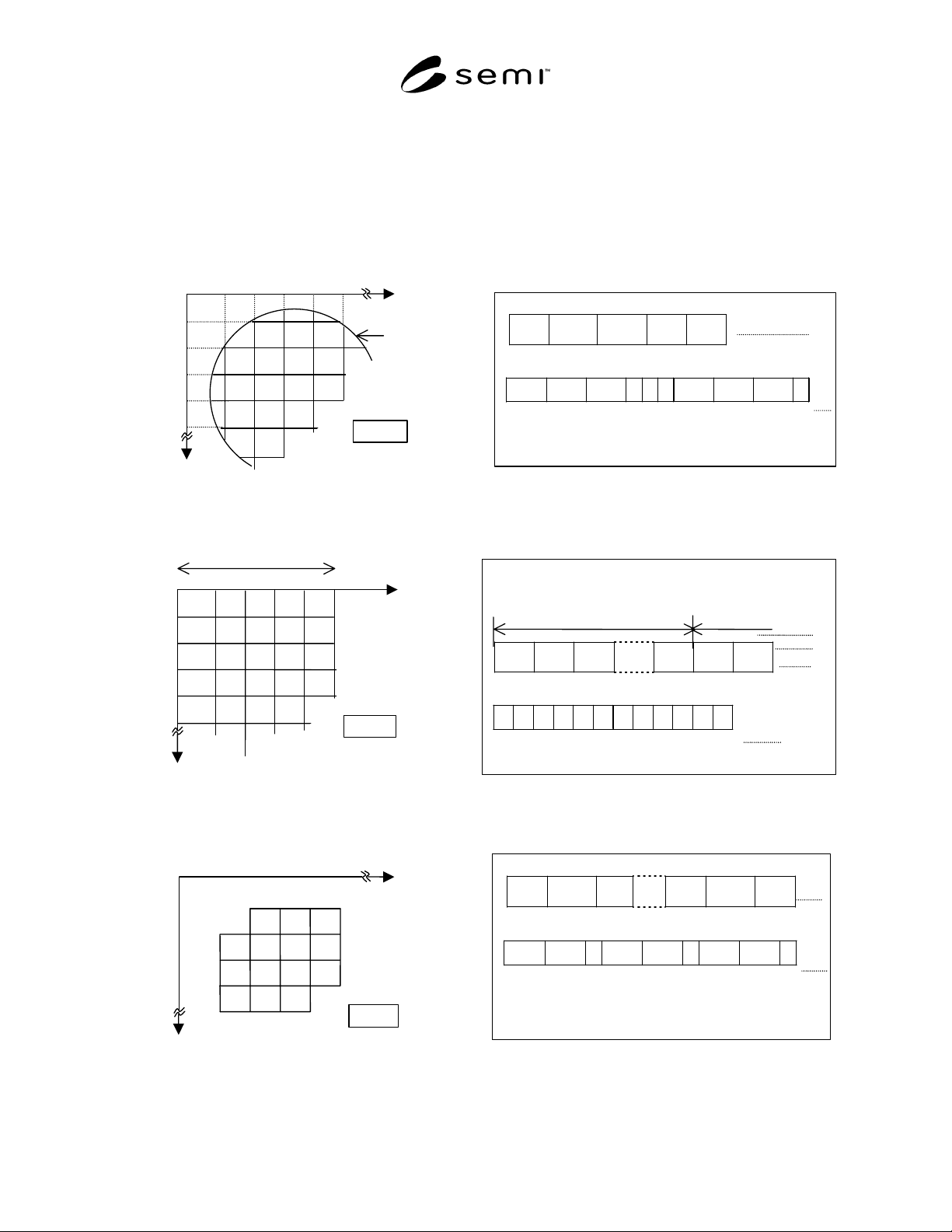
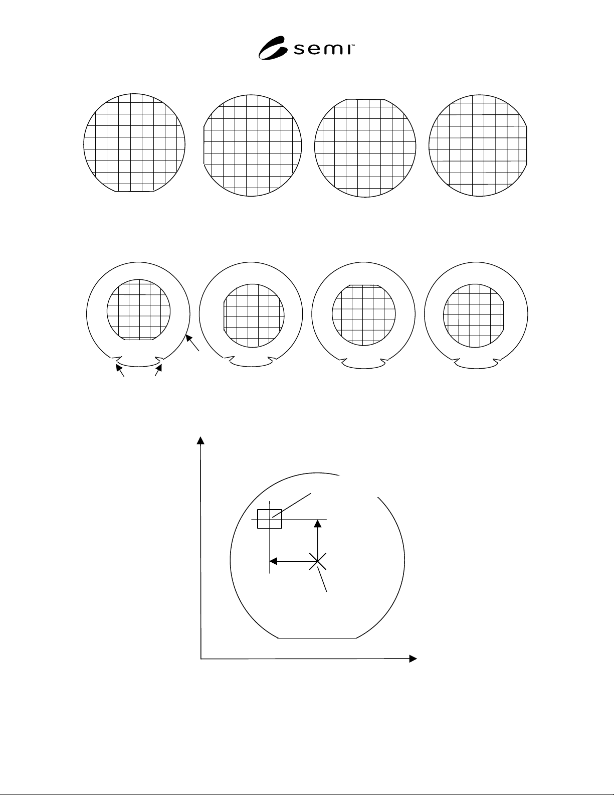
A1-1 This appendix shows how the map data items may be applied to wafers as well as some additional information
specific to this substrate type. See Figures A1-1 through A1-8.
ORIGIN
Column
Row
0
1234
0
1
2
3
4
WAFER
3
3
3
31
1
1
1
NUMBER:BIN DATA
2
2
2
2
2
2
DATA STRUCTURE
Col.
Row.
CHIP
QTY.
Bin Bin
DATA EX.
0002 0001 0003 3 1 3 0001 0002 0004 3
1
Figure A1-1a
Row/Column Format (MapType = “Row”)
ORIGIN
Column
Row
01 234
0
1
2
3
4
3
2
3
31
1
1
1
NUMBER:BIN DATA
2
2
2
2
2
2
DATA STRUCTURE
Bin
Bin Bin … Bin Bin Bin
DATA EX.
000000031303
1
COLUM NUMBER=5
00
00
0
00
0
0
0
Row=0
Col=0 Col=1 Col=2 Col=0
Col=1
Col=n
Row=1
Figure A1-1b
Array Format (MapType = “Array”)
Row
01234
0
1
2
3
4
1
1
1
1
NUMBER:BIN DATA
2
2
22
2
2
DATA STRUCTURE
Col.
Row. Bin … Col. Row. Bin
DATA EX.
0002 0001 3 0003 0001 1 0004 0001 2
Column
ORIGIN
3
3
2
3
Figure A1-1c
Coordinate Format (MapType = “Device”)
SEMI G81-0703 © SEMI 2000, 2003 8
0 deg. 90 deg. 180 deg. 270 deg.
Figure A1-2
Orientation of the Wafer Flat or Notch (Orientation)
FILM
FRAME
NOTCH
0 deg. 90 deg. 180 deg. 270 deg.
Figure A1-3
Orientation of the Wafer Flat or Notch on the Film Frame
+Y
+X
WAFER CENTER
REFERENCE CHIP CENTER
-x
y
Figure A1-4
Reference Device Position (RefDevicePosX and RefDevicePosY)