semi合集-English.pdf - 第4212页
SEMI F73-1102 © SEMI 2002 14 1 5 6 7 10 11 12 13 9 8 2 B D C E F H G J I K L M N O P Q S R TU 3 4 14 A 15 16 Figure A2-6 Long, Partially Continuous St ringer; the Inclusion that Formed this Stringer has been Electropoli …
SEMI F73-1102 © SEMI 2002 13
1
5
6
7
10
11
12
13
9
8
2
B DC E
F
HG
JI KL
M
NOPQ SR TU
3
4
14
A
15
16
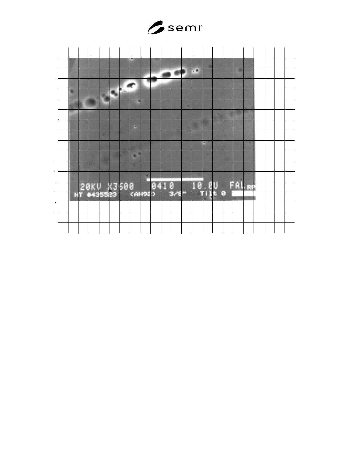
Figure A2-5
Pits Left by Inclusion Stringers in Which the Inclusions Have Been Electropolished Out; Also Numerous
Discrete Pits. All Pits with Edges Distinct Enough to Image with a “White Halo” Effect are Countable. This
Includes All of the Pits Associated with the Upper Stringer, and Those in the Lower Stringer in Grids M7N7,
O6 and O7, P6, Q6, R5 and R6. Also G1, Q1, A4, G5, L5, G7, N9, R9, G10, H12, Q12, E13, J13, N14, O14.
SEMI F73-1102 © SEMI 2002 14
1
5
6
7
10
11
12
13
9
8
2
B DC E
F
HG
JI KL
M
NOPQ SR TU
3
4
14
A
15
16
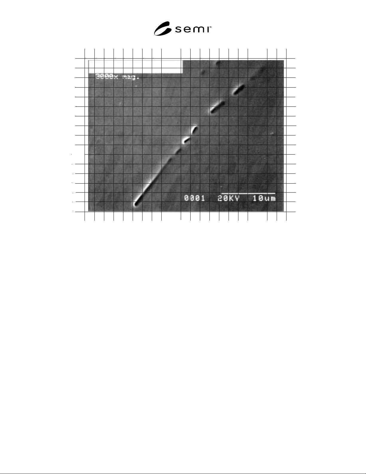
Figure A2-6
Long, Partially Continuous Stringer; the Inclusion that Formed this Stringer has been Electropolished Out.
All Grids Occupied by the Stringer Should be Counted, from F16 to S2. Also Pits at M2, N1 and O1.
SEMI F73-1102 © SEMI 2002 15
1
5
6
7
10
11
12
13
9
8
2
B DC E
F
HG
JI KL
M
NOPQ SR TU
3
4
14
A
15
16
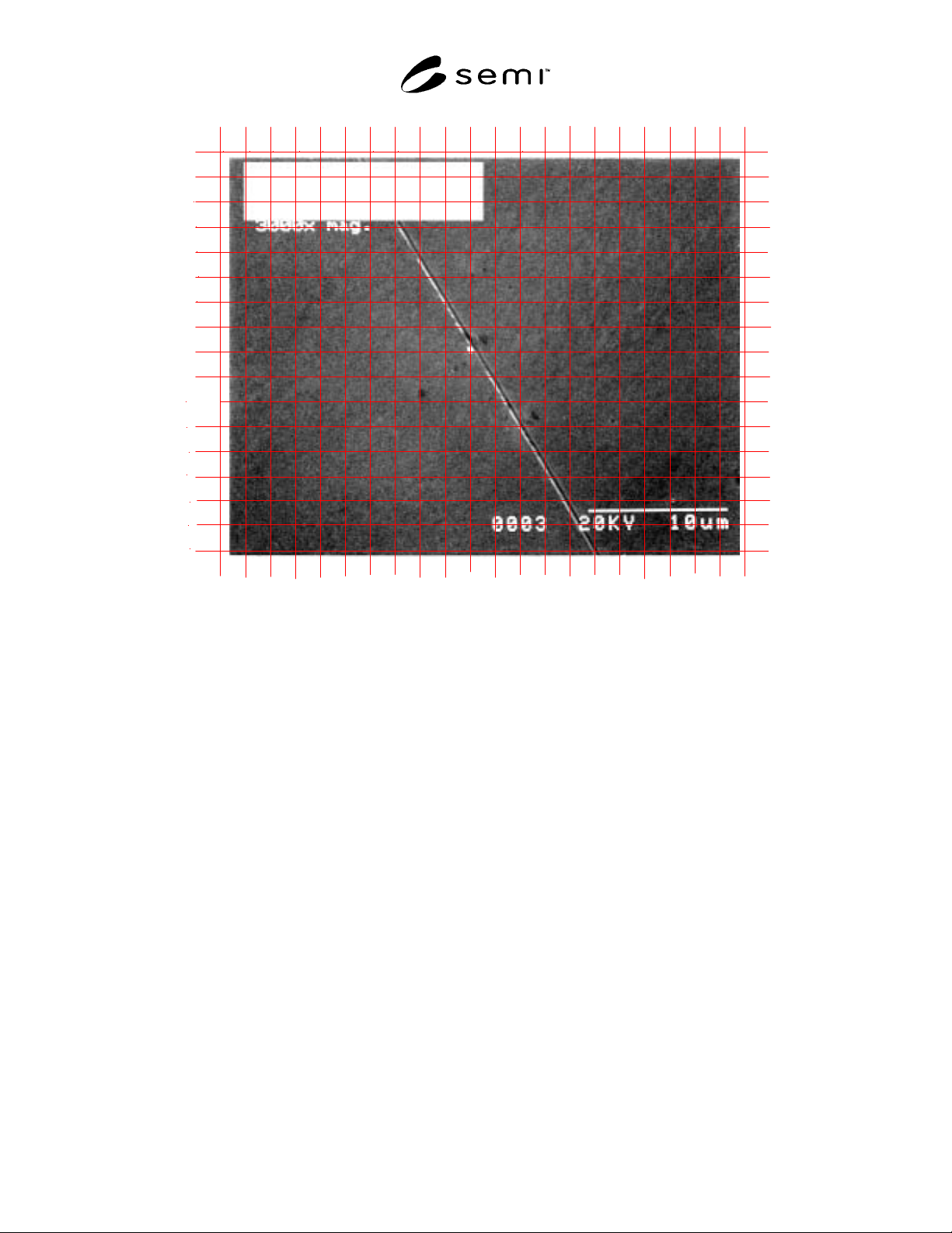
Figure A2-7
Scratch Counted in Grids H3-5, I5 and 6, J7 and 8, K8-10, L10 and 11, M12 and 13, N13-15, O15 and 16.
Pits Counted in Grids J9, H10, I10, M11.
NOTICE: SEMI makes no warranties or representations as to the suitability of the standards set forth herein for any
particular application. The determination of the suitability of the standard is solely the responsibility of the user.
Users are cautioned to refer to manufacturer' s instructions, product labels, product data sheets, and other relevant
literature, respecting any materials or equipment mentioned herein. These standards are subject to change without
notice.
By publication of this standard, Semiconductor Equipment and Materials International (SEMI) takes no position
respecting the validity of any patent rights or copyrights asserted in connection with any items mentioned in this
standard. Users of this standard are expressly advised that determination of any such patent rights or copyrights, and
the risk of infringement of such rights are entirely their own responsibility.
Copyright by SEMI® (Semiconductor Equipment and Materials
International), 3081 Zanker Road, San Jose, CA 95134. Reproduction o
f
the contents in whole or in part is forbidden without express written
consent of SEMI.