semi合集-English.pdf - 第5336页
SEMI M51-0303 © SEMI 2002, 2003 14 0 0.2 0.4 0.6 0.8 1 1.2 0 20 40 60 80 100 E ste p (MV/cm) B-mode ratio (%) Tox: 25 nm S: 10 mm 2 High Middle Low Figure R1-4 B-mode Failure Percent vs. Step Height of the Electric Field…
SEMI M51-0303 © SEMI 2002, 2003 13
R1-1.3.6 On the other hand, too high a stepping-up of
the applied electric field stress, for example, 1.0
MV/cm or more, leads to broadening of the dielectric
breakdown electric field. That is, the reliability of the
measurement result is decreased.
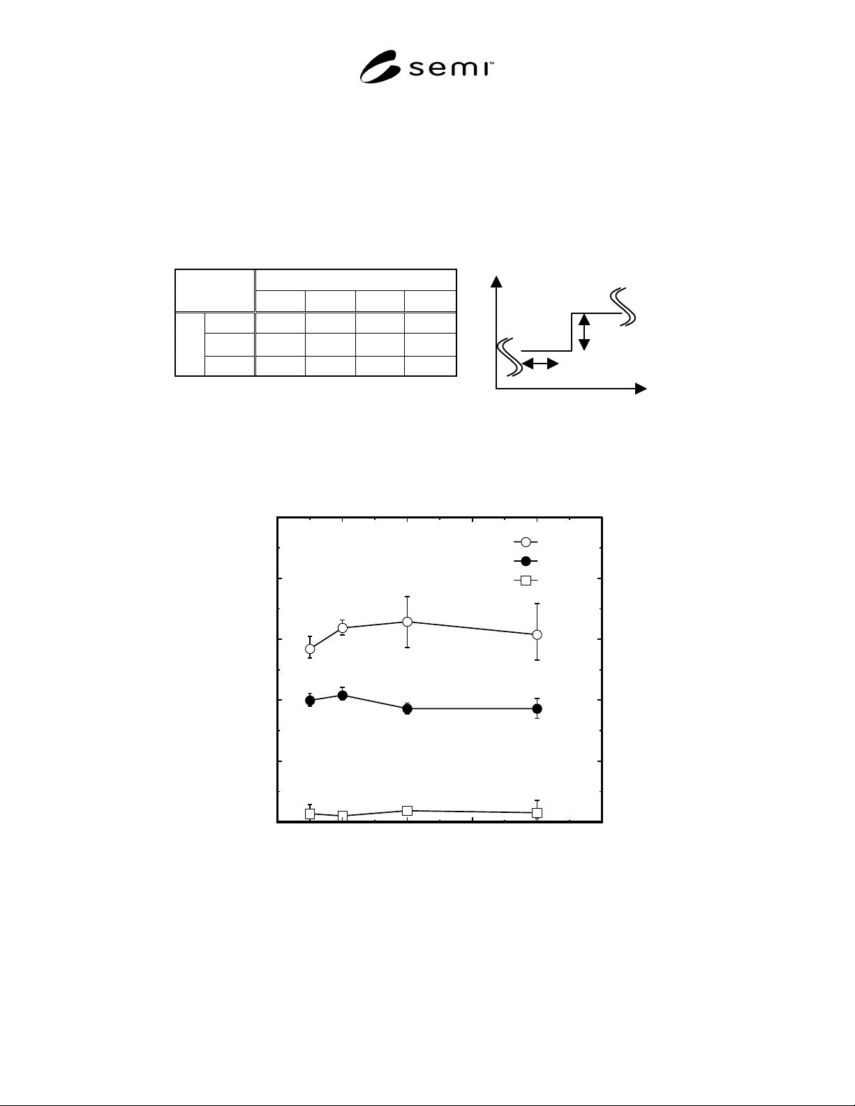
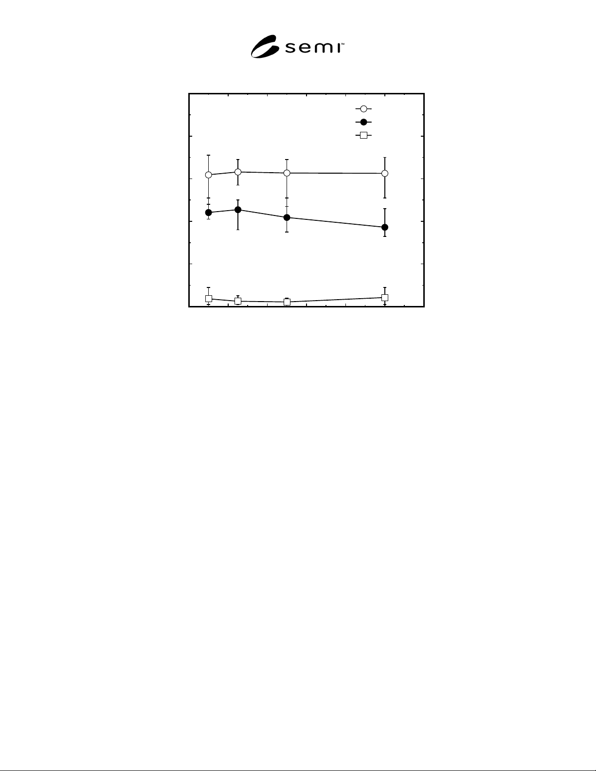
R1-1.3.7 In this round robin as shown in Figure R1-4,
the B-mode failure percent did not depend on the step
height of the applied electric field stress with a hold
time of 200 ms. An electric field step height of 0.1-0.5
MV/cm did not cause any problems in the measurement
results. Therefore, considering the above practical
factors, a step height range of 0.1–0.5 MV/cm, and
especially, 0.25 MV/cm are recommended.
TZDB(Step Voltage)
a) Group I: B, D, E b) Group II: A, F
E
step
(MV/cm)
0.1 0.25 0.5 1.0
100 I I - -
200 II I
*
, II II II
T
hold
(ms)
800 - I I -
(* E measured T
hold
= 400ms)
E
step
T
hold
Judgement Current:10
-5
A
E
T
Figure R1-2
Applied Gate Electric Field Stress Condition in TZDB and Measurement Group Division
0 0.2 0.4 0.6 0.8 1
0
20
40
60
80
100
T
hold
(s)
B-mode ratio (%)
Tox: 25 nm
S: 10 mm
2
High
Middle
Low
Figure R1-3
B-Mode Failure Percent vs. Hold Time of Applied Electric Field Stress with a Step Height of 0.25 MV/cm in
TZDB
SEMI M51-0303 © SEMI 2002, 2003 14
0 0.2 0.4 0.6 0.8 1 1.2
0
20
40
60
80
100
E
ste
p
(MV/cm)
B-mode ratio (%)
Tox: 25 nm
S: 10 mm
2
High
Middle
Low
Figure R1-4
B-mode Failure Percent vs. Step Height of the Electric Field Stress with a Hold Time of 200 ms in TZDB
NOTICE: SEMI makes no warranties or representations as to the suitability of the standards set forth herein for any
particular application. The determination of the suitability of the standard is solely the responsibility of the user.
Users are cautioned to refer to manufacturer's instructions, product labels, product data sheets, and other relevant
literature, respecting any materials or equipment mentioned herein. These standards are subject to change without
notice.
By publication of this standard, Semiconductor Equipment and Materials International (SEMI) takes no position
respecting the validity of any patent rights or copyrights asserted in connection with any items mentioned in this
standard. Users of this standard are expressly advised that determination of any such patent rights or copyrights, and
the risk of infringement of such rights are entirely their own responsibility.
Copyright by SEMI® (Semiconductor Equipment and Materials
International), 3081 Zanker Road, San Jose, CA 95134. Reproduction o
f
the contents in whole or in part is forbidden without express written
consent of SEMI.

SEMI M52-0703 © SEMI 2002, 2003 1
SEMI M52-0703
GUIDE FOR SPECIFYING SCANNING SURFACE INSPECTION
SYSTEMS FOR SILICON WAFERS FOR THE 130-nm TECHNOLOGY
GENERATION
This guide was technically approved by the Global Silicon Wafer Committee and is the direct responsibility
of the European Silcon Wafer Committee. Current edition approved by the European Regional Standards
Committee on April 3, 2003. Initially available at www.semi.org June 2003; to be published July 2003.
Originally published November 2002; previously published March 2003.
1 Purpose
1.1 This guide provides recommendations for
specifying Scanning Surface Inspection Systems
(SSIS) for the 130-nm technology generation. The
number and size of localized light scatterers (LLS) on
silicon wafers are specified by customers of silicon
wafer suppliers and are usually part of Certificates of
Compliance. Suppliers of silicon wafers and their
customers might measure these parameters using
equipment provided by different manufacturers of such
equipment or using different generations of equipment
from one supplier. Therefore, standardization of
various aspects of such measurement equipment both
improves data exchange and data interpretation and aids
in procurement of appropriate tools.
2 Scope
2.1 This guide outlines and recommends basic
specifications for SSIS equipment used for the 130-nm
technology generation as driven by the International
Technology Roadmap for Semiconductors: 1999
edition (ITRS)
1,2
and in the forecasts of the major
manufacturers of semiconductor devices.
NOTE 1: Future revisions of this Guide are expected to
reflect changed requirements for the 130-nm node as well as
requirements of other nodes.
2.2 The guide applies to measurement equipment used
for verifying the quality parameter LLS counts per
wafer in large scale production of bare polished or
epitaxial surfaces of silicon wafers, the back surface of
which may be polished or acid etched either bare or
covered by an unpatterned, homogeneous layer of
polysilicon or LTO (low temperature oxide). Artifacts
(e.g reference materials) for calibrating measurement
equipment might have different properties.
2.3 The guide also applies to measurement equipment
that provides only a subset of the measurement features
outlined in Table 3.
1 SEMATECH, 2706 Montopolis Drive, Austin, TX 78741-6499,
USA Website : www.sematech.org
2 More recent versions of the ITRS are available from the homepage
of International SEMATECH: www.sematech.org
NOTICE: This standard does not purport to address
safety issues, if any, associated with its use. It is the
responsibility of the users of this standard to establish
appropriate safety health practices and determine the
applicability of regulatory or other limitations prior to
use.
3 Limitations
3.1 This guide does not apply to measurement
equipment used to control intermediate process steps
during silicon wafer manufacturing. However, it may
be completely or partly used for measurement
equipment for those applications provided
corresponding constraints are appropriately identified.
3.2 This guide does not apply to measurement
equipment for SOI wafers (Silicon on Insulators) or
patterned wafers.
4 Referenced Standards
4.1 SEMI Standards
SEMI E1.9 — Mechanical Specification for Cassettes
Used to Transport and Store 300 mm Wafers
SEMI E5 — SEMI Equipment Commuications
Standard 2 Message Content (SECS-II)
SEMI E10 — Specifcation for Definition and
Measurement of Equipment Reliability, Availability,
and Maintainability (RAM)
SEMI E19 — Standard Mechanical Interface (SMIF)
SEMI E30 — Generic Model for Communications and
Control of Manufacturing Equipment (GEM)
SEMI E37 — High Speed SECS Message Services
(HSMS) Generic Services
SEMI E47 — Specification for 150 mm/200 mm Pod
Handles
SEMI E47.1 — Provisional Mechanical Specification
for Boxes and Pods Used to Transport and Store 300
mm Wafers