semi合集-English.pdf - 第167页
SEMI E21-94 © SEMI 1991, 2002 7 RELATED INFORMATION 1 NOTE: This related information is not an official part of SEMI E21 but was reapproved for public ation by full letter ballo t procedures on July 21, 2002. R1-1 Transp…
SEMI E21-94 © SEMI 1991, 2002 6
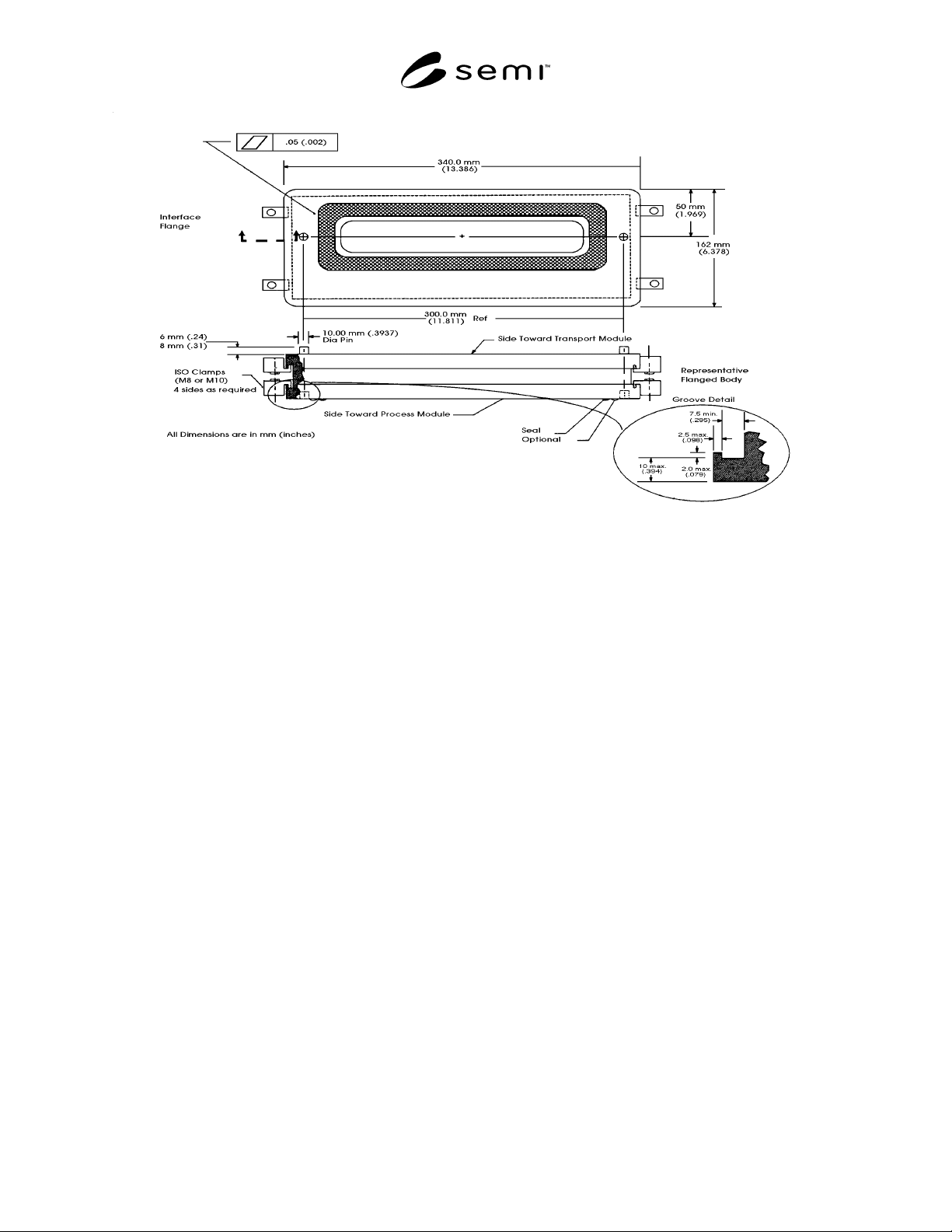
Figure 4
Flange Specification

SEMI E21-94 © SEMI 1991, 2002 7
RELATED INFORMATION 1
NOTE: This related information is not an official part of SEMI E21 but was reapproved for publication by full letter ballot
procedures on July 21, 2002.
R1-1 Transport Module Reach
R1-1.1 The reach (see Section 4.1.1) permits a wafer of
200 mm (8 in.) diameter or smaller to be placed on a
wafer support platform in a process chamber with
allowance for the optional isolation valve on the
process module and the chamber wall thickness. The
substantial clearance between the wafer and the
chamber wall is to allow freedom for process-specific
design requirements.
R1-1.2 Individual process chamber designs may place
the wafer closer to the interface plane than 305 mm (12
in.) and still conform to the standard.
R1-1.3 Wafers are transported individually in a
horizontal attitude. Modules may contain any number
of wafers. For example, batch processing is allowed.
R1-2 Vertical Position of Transport Plane
R1-2.1 The transport plane elevation of 1100 mm
(43.307 in.) (see Section 4.1.2) is positioned within the
constraints placed on the cluster tool by the Inter-
Equipment Automation requirement for cassette
placement (SEMI E15). SEMI E15 specifies the load
height for cassettes to be 900 mm (35.46 in.) ± 10 mm
(0.394 in.) outside an environmental load-lock.
R1-2.2 The vertical position of the transport plane is
derived from the following contributions:
• 910 mm (35.854 in.) is a worst-case cassette load
height position.
• 12 mm (0.473 in.) is a nominal pickup clearance to
zero a wafer elevator indexer after the cassette is
drawn into the environmental load-lock.
• 178 mm (7.01 in.) is the location of the top slot in a
standard 200 mm (8 in.) wafer carrier (SEMI E1.7).
R1-2.3 These additive contributions assure that the
transport plane elevation allows as much space as
possible for location of support equipment such as
pumps, electronics, and power supplies below the
process chamber. The 1100 mm (43.307 in.) “nominal”
dimension could be adjustable by the module(s) to
within ± 25 mm (1 in.).
R1-3 Vertical Motion
R1-3.1 The standard (see Section 4.1.2.1) requires that
the transport module be capable of moving in two
planes. An ability to move in other planes is optional.
R1-3.2 The transport module moves the wafer in the
horizontal wafer transport plane (see Definition 3.12).
The transport module has a vertical motion capability
for wafer handoff or pickup. It is assumed that the
transport module moves in the lower plane after wafer
handoff or prior to wafer pickup.
R1-4 Interface Seal Zone
R1-4.1 The interface seal zone (see Section 4.2.1) is
sufficiently wide to permit double seals with
intermediate pumping.
R1-4.2 Blank-Off Plates — The location of the seals on
the transport module allows plain blank-off plates to be
used for environmental sealing.
R1-5 Wafer Transport Zone
R1-5.1 The minimum specified height of 32 mm
(1.184 in.) (see Section 4.2.2) provides sufficient
clearance for passage of a knuckle joint or pivot point
in the transport module end effector (see SEMI E22,
" Cluster Tool Module Interface: Transport Module End
Effector Exclusion Volume Standard" ) and for 6 mm
(0.238 in.) of vertical motion. The wafer transport zone
may be expanded up to the boundary of the interface
seal zone when a module requires a larger opening (see
Section 4.2.1 and Figure 3).
R1-6 Interface Plane Alignment Pins
R1-6.1 The standard (see Section 4.2.3) implies the
normal engineering practice of chamfering pin ends and
countersinking pin locating holes. Actual dimensions
for this have been specified or recommended by other
authorities.
R1-6.2 Pins reside in the sealing surface to avoid
accidental damage to the surface finish during assembly
and disassembly. With centrally placed pins, valves
may be mounted in either orientation if this simplifies
servicing or accessibility.
R1-6.3 A clearance hole and slot arrangement allows
use of dissimilar flange materials in a dynamic thermal
environment.
R1-7 Isolation Valves
R1-7.1 The standard (see Section 4.2.4) allows the
valves to be integral to the modules or discrete
separable units.
SEMI E21-94 © SEMI 1991, 2002 8
R1-8 Clamping
R1-8.1 The standard (see Section 4.3.1) allows a
universal clamping scheme to be employed. Claw
clamps designed for use with ISO flanges are
accommodated by the use of a perimeter groove around
the flange.
R1-8.2 The clamping scheme provides several benefits:
• Independence from any hole pattern requirements.
• Flanges may be connected to flat plates or to other
flanges.
• The number of clamps and the number of sides
used to draw the flanges together may be varied as
required by the compression forces necessary for
the sealing method used. For example, clamps may
be spaced on 30 mm (1.191 in.) centers for metal
seals and on 150 mm (6 in.) centers for elastomeric
seals.
• Any type of clamp may be used that accommodates
the perimeter groove.
NOTICE: SEMI makes no warranties or
representations as to the suitability of the standards set
forth herein for any particular application. The
determination of the suitability of the standard is solely
the responsibility of the user. Users are cautioned to
refer to manufacturer' s instructions, product labels,
product data sheets, and other relevant literature,
respecting any materials or equipment mentioned
herein. These standards are subject to change without
notice.
By publication of this standard, Semiconductor
Equipment and Materials International (SEMI) takes no
position respecting the validity of any patent rights or
copyrights asserted in connection with any items
mentioned in this standard. Users of this standard are
expressly advised that determination of any such patent
rights or copyrights, and the risk of infringement of
such rights are entirely their own responsibility.
Copyright by SEMI® (Semiconductor Equipment and Materials
International), 3081 Zanker Road, San Jose, CA 95134. Reproduction o
f
the contents in whole or in part is forbidden without express written
consent of SEMI.