semi合集-English.pdf - 第5321页
SEMI M50-1104 © SEMI 2001, 2004 7 A1-7 Apparatus A1-7.1 SSI S under test — as define d in Section 7 of this standard with ch aracteristics as outlined in SEMI M53. A1-8 Reference Wafer A1-8.1 The refe rence wafer shall m…

SEMI M50-1104 © SEMI 2001, 2004 6
APPENDIX 1
DEFAULT PROCEDURE FOR DETERMINATION OF SCANNER XY
UNCERTAINTY
NOTICE: The material in this appendix is an official part of SEMI M50 and was approved by full letter ballot
procedures on April 22, 2004 by the North American Regional Standards Committee.
A1-1 Purpose
A1-1.1 This procedure is intended to be used for determining the scanner XY uncertainty for the scanning surface
inspection system (SSIS) under test when this information is not otherwise available.
A1-2 Scope
A1-2.1 This appendix covers a procedure for determining ability of an SSIS to report the location of a localized
light scatterer (LLS) on a silicon wafer surface under repeatability conditions.
NOTICE: This appendix does not purport to address safety issues, if any, associated with its use. It is the
responsibility of the users of this procedure to establish appropriate safety health practices and determine the
applicability of regulatory or other limitations prior to use.
A1-3 Limitations
A1-3.1 If particles are used as the reference LLSs, care must be taken both to avoid contamination by interfering
particles and to avoid removal of the reference particles.
A1-4 Referenced Standards
A1-4.1 SEMI Standards
SEMI E89 — Guide for Measurement System Capability Analysis
SEMI M1 — Specification for Monocrystalline Polished Silicon Wafers
SEMI M20 — Specification for Establishing a Wafer Coordinate System
SEMI M53 — Practice for Calibrating Scanning Surface Inspection Systems Using Certified Depositions of
Monodisperse Polystyrene Latex Spheres on Unpatterned Semiconductor Wafer Surfaces
NOTICE: Unless otherwise indicated, all documents cited shall be the latest published versions.
A1-5 Terminology
A1-5.1 Terms related to SSIS operation are defined in Section 5 of this standard and in SEMI M53.
A1-5.2 Terms related to uncertainty and repeatability are defined in SEMI E89.
NOTE 1: The current edition of SEMI M89 defines the repeatability used in this procedure as “static repeatability.”
A1-6 Summary of Procedure
A1-6.1 A reference silicon wafer with at least ten identifiable and stable LLSs (relatively large, isolated particles or
pits) located on its polished surface is scanned ten times by the SSIS under test without removing it from the SSIS
between scans.
A1-6.2 For each scan, a map of the positions associated with the specified laser light scattering events arising from
scattering from the LLSs on the wafer surface is obtained and the coordinates of these events are recorded.
A1-6.3 The coordinate data set is filtered to remove coordinates not associated with the selected LLSs.
A1-6.4 The sample standard deviations (x and y) are used to estimate the repeatability of the reported locations, and
the scanner XY uncertainty is calculated as the quadrature sum of the x- and y-sample standard deviations.
SEMI M50-1104 © SEMI 2001, 2004 7
A1-7 Apparatus
A1-7.1 SSIS under test — as defined in Section 7 of this standard with characteristics as outlined in SEMI M53.
A1-8 Reference Wafer
A1-8.1 The reference wafer shall meet the dimensional requirements of SEMI M1 for the largest diameter of wafer
to be inspected by the SSIS under test.
A1-8.2 The surface of the reference wafer shall contain at least ten LLSs (particles or pits) of a size (LSE) well
above the threshold, so that the capture rate is ~100%.
A1-8.3 These ten or more LLSs must be distributed over the entire surface of the wafer.
A1-9 Procedure
A1-9.1 Load the reference wafer into the SSIS with the fiducial (flat or notch) located in accordance with
customary operating procedures of the laboratory conducting the test.
A1-9.2 Scan the wafer and create a data set containing the reported x and y coordinates of each of the ten or more
selected LLSs.
A1-9.3 Call this scan, Scan 1.
A1-9.4 Repeat the scans, nine more times, and create nine more data sets containing the reported x and y
coordinates of each of the ten or more selected LLSs.
A1-10 Calculations
A1-10.1 Examine each of the data sets (either as wafer maps or mathematically) to determine that coordinate pairs
for each of the ten or more LLSs being analyzed appear in each of the ten scans.
A1-10.2 Delete from the data any coordinate pair that does not appear in all ten data sets.
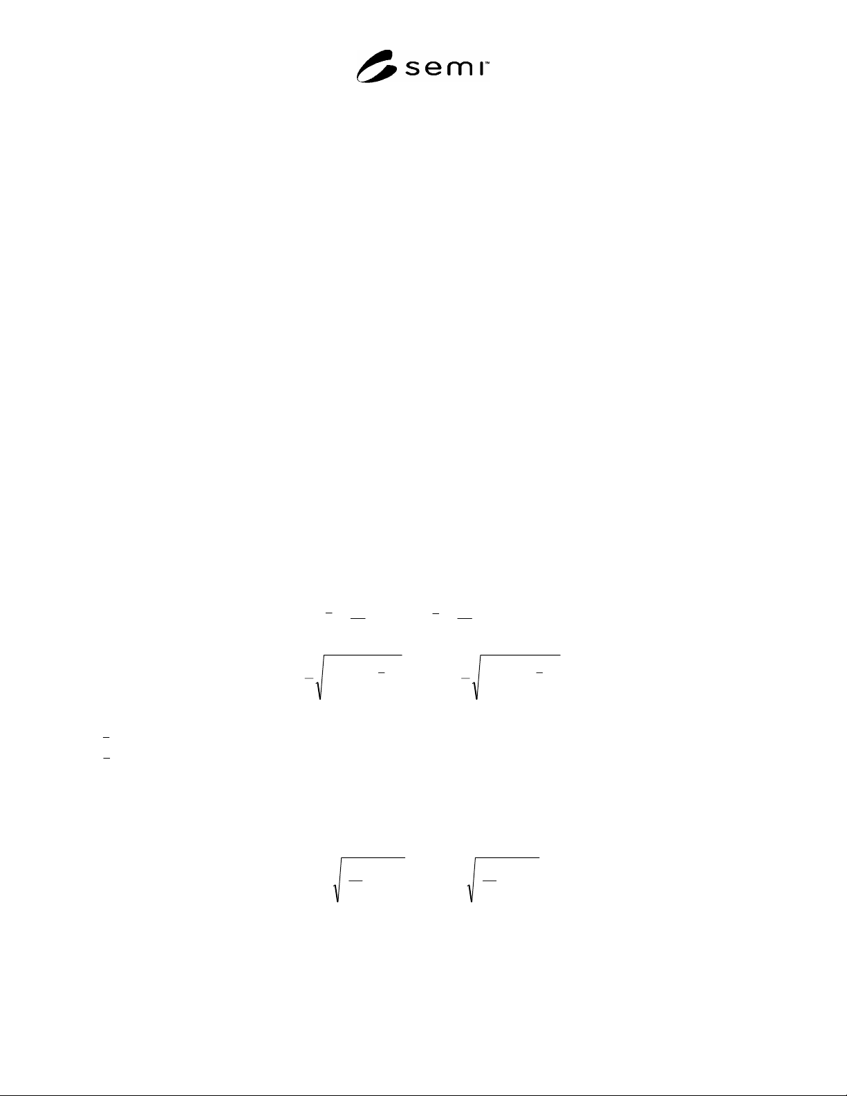
A1-10.3 Determine the average and the sample standard deviation of x and y coordinates of each of the N remaining
coordinate pairs as follows:
10
1
10
1
k
iki
xx and
10
1
10
1
k
iki
yy (A1)
10
1
2
)(
3
1
k
iikxi
xxs
and
10
1
2
)(
3
1
k
iikyi
yys
(A2)
where:
i
x
= average of the ten x coordinates reported for the i
th
LLS,
i
y
= average of the ten y coordinates reported for the i
th
LLS,
s
xi
= sample standard deviation of the ten x coordinates reported for the i
th
LLS,
s
yi
= sample standard deviation of the ten y coordinates reported for the i
th
LLS, and
k = scan number (from 1 to 10).
A1-10.4 Calculate the pooled sample standard deviations of the reported x and y coordinates as follows:
N
i
xix
s
N
S
1
2
1
and
N
i
yiy
s
N
S
1
2
1
(A3)
where:
S
x
= pooled sample standard deviation of the ten x coordinates reported for the N LLSs,
S
y
= pooled sample standard deviation of the ten y coordinates reported for the N LLSs, and
N = number of coordinate pairs appearing in all ten scans.
SEMI M50-1104 © SEMI 2001, 2004 8
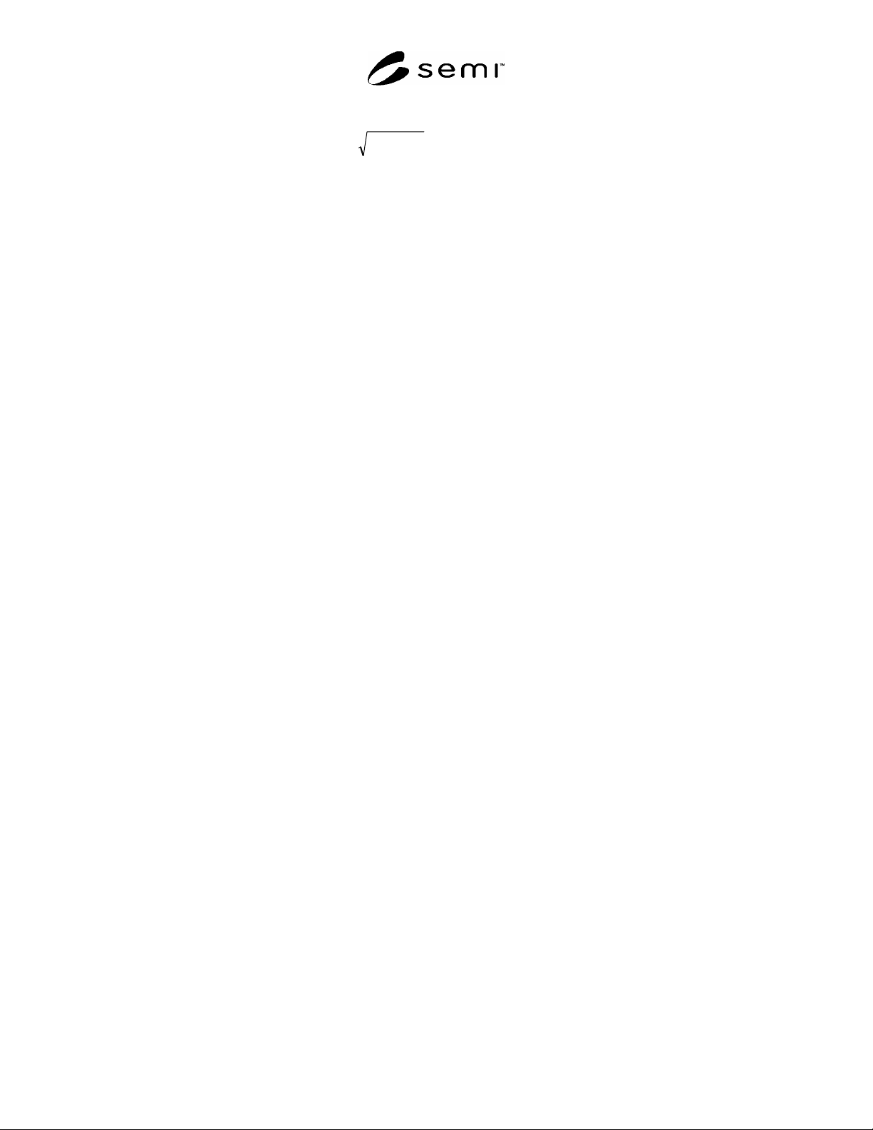
A1-10.5 Calculate and record the scanner XY uncertainty as follows:
)(
22
yx
SSS (A4)
NOTICE: SEMI makes no warranties or representations as to the suitability of the standards set forth herein for any
particular application. The determination of the suitability of the standard is solely the responsibility of the user.
Users are cautioned to refer to manufacturer's instructions, product labels, product data sheets, and other relevant
literature, respecting any materials or equipment mentioned herein. These standards are subject to change without
notice.
By publication of this standard, Semiconductor Equipment and Materials International (SEMI) takes no position
respecting the validity of any patent rights or copyrights asserted in connection with any items mentioned in this
standard. Users of this standard are expressly advised that determination of any such patent rights or copyrights, and
the risk of infringement of such rights are entirely their own responsibility.
Copyright by SEMI® (Semiconductor Equipment and Materials
International), 3081 Zanker Road, San Jose, CA 95134. Reproduction of
the contents in whole or in part is forbidden without express written
consent of SEMI.