semi合集-English.pdf - 第5754页
SEMI P19-92 © SEMI 19 92, 1996 5 across th e ends) is provided on the array to allow recognition of the cell as a unit. 3.2.7 Electr ical Cell — (See Figure 1 2. ) 3.2.7.1 The electrical cell is des igned t o provide ver…
SEMI P19-92 © SEMI 1992, 1996 4
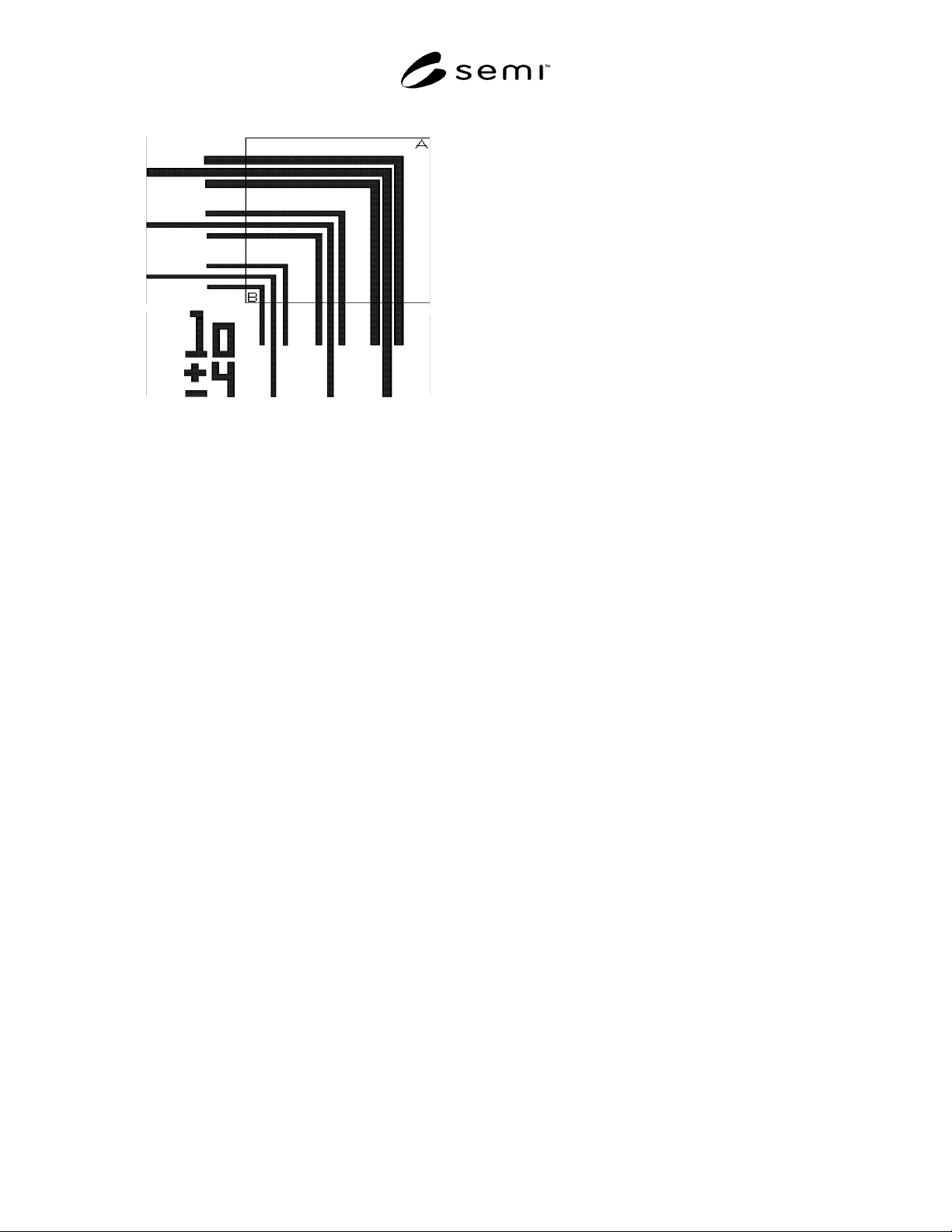
Figure 7
The square area, shown above, is removed to create
straight-line cell.
3.2.2.2 To create the straight-line cell from the L-bar
cell, the area removed will be a square defined by two
diagonal corners referred to as “A” and “B” in Figure 7.
Corner “A” is the outer edge of the outermost elbow.
Corner “B” is a point inside the innermost elbow whose
distance to the nearest edge is five times that of the
smallest CD — or 5.0 µm if the smallest CD is less than
1.0 µm. This square area must remain unpatterned.
3.2.3 Proximity Dagger Cell — (See Figure 8.)
3.2.3.1 The proximity dagger cell is designed to
provide information on the proximity effects of isolated
lines/spaces in relation to large area blocks. This cell
design allows clear and dark features to be measured
simultaneously in one layout.
3.2.3.2 The design elements within the cell are the
nominal feature linewidth, the nominal feature
spacewidth, and the staircase stepwidth. The stepwidth
is user-selected, but it is recommended to be at least
25% of the nominal feature pitch (i.e., pitch equals
nominal linewidth plus nominal spacewidth).
3.2.3.3 The cell consists of a nine-tier staircase
reproduced symmetrically in both clear and darkfields.
A full description of the clearfield staircase (i.e., large
chrome islands) is given. The same descriptions apply
for the darkfield staircase except the polarities are
reversed. Each tier is 10 microns tall. The full width of
the cell is 40 microns and the full height is 180 microns.
The first tier separates the nominal feature width
symmetrically from the large chrome islands by an
amount equal to the nominal width. Tiers 2–7 are
successively wider by the indicated bias. The 8th and
9th tiers will be 5 and 10 times the nominal feature
width respectively.
3.2.4 Contact Array Cell — (See Figure 9.)
3.2.4.1 The contact array cell is desig ned to provide
resolution and proximity-effect information over a wide
range of contact sizes.
3.2.4.2 The design elements are the no minal square
contact dimension, the inter-contact dimension within
the 5 × 5 and the 3 × 3 arrays. The latter dimension
will be equal to the contact dimension.
3.2.4.3 The contact array cell will consist of three
subgroups: a 5 × 5 contact array, a 3 × 3 contact array,
and an isolated contact. The 5 × 5 array will produce
the maximal proximity (i.e., dense printing) for the
center contact. The center contact in the 3 × 3 array
will exhibit proximal printing effects different from
both the isolated contact and the dense contact.
3.2.5 Staggered Contact Array — (See Figure 10.)
3.2.5.1 The staggered contact array ce ll is designed to
improve the probability of cross-sectioning small
contacts for SEM metrology analysis.
3.2.5.2 The design elements are the sq uare contact
dimension, the column-to-column vertical offset — or
staggering — and the contact-to-contact spacing. The
contact-to-contact spacing will be equal to the square
contact dimension.
3.2.5.3 The contacts are laid out using a minimum of
three columns of contacts. The user-selected offset
between columns should allow the contacts to remain
on grid.
3.2.5.4 The lines (or spaces) shown on the left side of
Figure 10 are optional. They have been placed to
provide feature identification of pitch calibration. If the
widths are to be submicron, 5 lines (or spaces) instead
of 3 will be required.
3.2.6 Linearity Cell — (See Figure 1 1.)
3.2.6.1 The linearity cell is designed to test (1) the
linearity of the measurement method, assuming the
lithographical process is linear over all line sizes used,
or (2) the linearity of the process, assuming that the
metrological method is linear over all line sizes used.
3.2.6.2 The design elements of this cell are the
linewidths, the interfeature spacing, and the minimum
line lengths. Unlike the other cells, its elements are not
adjusted to a nominal critical dimension, but rather are
numerically specified as constants for all applications.
3.2.6.3 The cell consists of nine parallel lines, placed
on a five-micron pitch. The linewidths are 1.2, 1.1, 1.0,
0.9, 0.8, 0.7, 0.6, 0.5, and 0.4 microns. The line lengths
are a minimum of ten microns. A two-micron top and
bottom border (running orthogonal to the parallel lines,
SEMI P19-92 © SEMI 1992, 19965
across the ends) is provided on the array to allow
recognition of the cell as a unit.
3.2.7 Electrical Cell — (See Figure 12.)
3.2.7.1 The electrical cell is designed to provide very
precise and relatively fast determinations of the average
linewidth of a conductive film using an automated test
system, but can also be used with a manual prober.
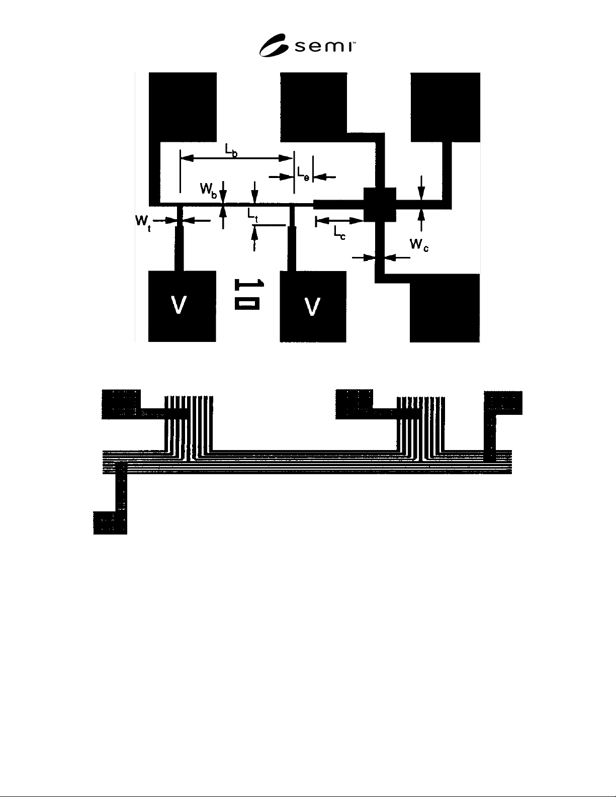
3.2.7.2 The design elements of this cell are the bridge
resistor linewidth, W
b
, the center-of-tap to center-of-tap
bridge length, L
b
, the sheet and bridge tap widths, W
c
and W
t
, the sheet and bridge tap lengths, L
c
and L
t
, the
extension of the bridge resistor line to the nearest
discontinuity in that line, L
e
, and the size of the square
sheet will be 35 – 100 µm. See Figure 13 for the
labeling of these elements. The rules for these elements
are as follows:
W
t
≤ W
b
(for L
b
< 100 W
b
)(1)
W
t
≤ 1.2*W
b
(for L
b
≥ 100 W
b
and W (2)
L
b
≥ 15W
b
for 80 µm, whichever is larger) (3)
L
t
> 2W
t
(4)
L
e
> 2W
b
(5)
L
c
> 2W
c
(6)
3.2.7.3 The cell consists of two types o f four-point
Kelvin structures: a van der Pauw sheet resistor and one
or more bridge resisitors. The orientation of the
individual bridge resistors is user-defined. The bridge
resisitors also can be surrounded by dummy lines to
measure the process bias due to proximity effect. On
structures containing the dummy lines, the
interconnects will hook up to the bridge resistor in a
perpendicular fashion, as shown in Figure 14.
3.2.7.4 The pad labeled with a V in Figures 13 and 15
will be used for voltage measurement only, and will be
used as the fourth point in the sheet resistivity
measurements that will be used to make the linewidth
determination.
SEMI P19-92 © SEMI 1992, 1996 6
Figure 13
Electrical Cell, 2 × n Configuration with Labeling
Figure 14
Blow-Up of Bridge Resistor with Proximity Lines