semi合集-English.pdf - 第940页
SEMI E119-1104 © SEMI 2002, 2004 12 be able to withstand a force in any direction of at least f 60. It is recom mended that SE MI E15.1 tool load ports be designed to accomm odate the minimum hole dimensions of the retai…
SEMI E119-1104 © SEMI 2002, 2004 11
x
42 = 50 ± 1
x
41 = 30 ± 1
y
45
= 65.3 ± 1
y
47
58
x
44
53
facial
datum
plane
bilateral
datum
plane
front side of
the FOBIT
where wafers
are accessed
y
41 = 30 ± 1
y
46
= 71 ± 1
x
43 = 50 ± 1
x
47
58
(16x)
= 45
± 0.5°
position
notch
orientation
notch
x
46 = 71 ± 1
x
45 =
65.3 ± 1
y
44
53
d63
= 35 ± 0.1
y
68
55
x
69 = 7.6 ± 0.1
= 60°
r63
66
top of
FOBIT
bilateral
datum plane
horizontal
datum plane
z
47
= 221 ± 1
position notch
d63
= 35 ± 0.1
cross-section
above:
x
69 = 7.6 ± 0.1
= 45 ± 1°
= 52 ± 1°
x
45 = 65.3 ± 1
x
46 = 71 ± 1
z
49
8
z48
15
z
50
5
r
59
6
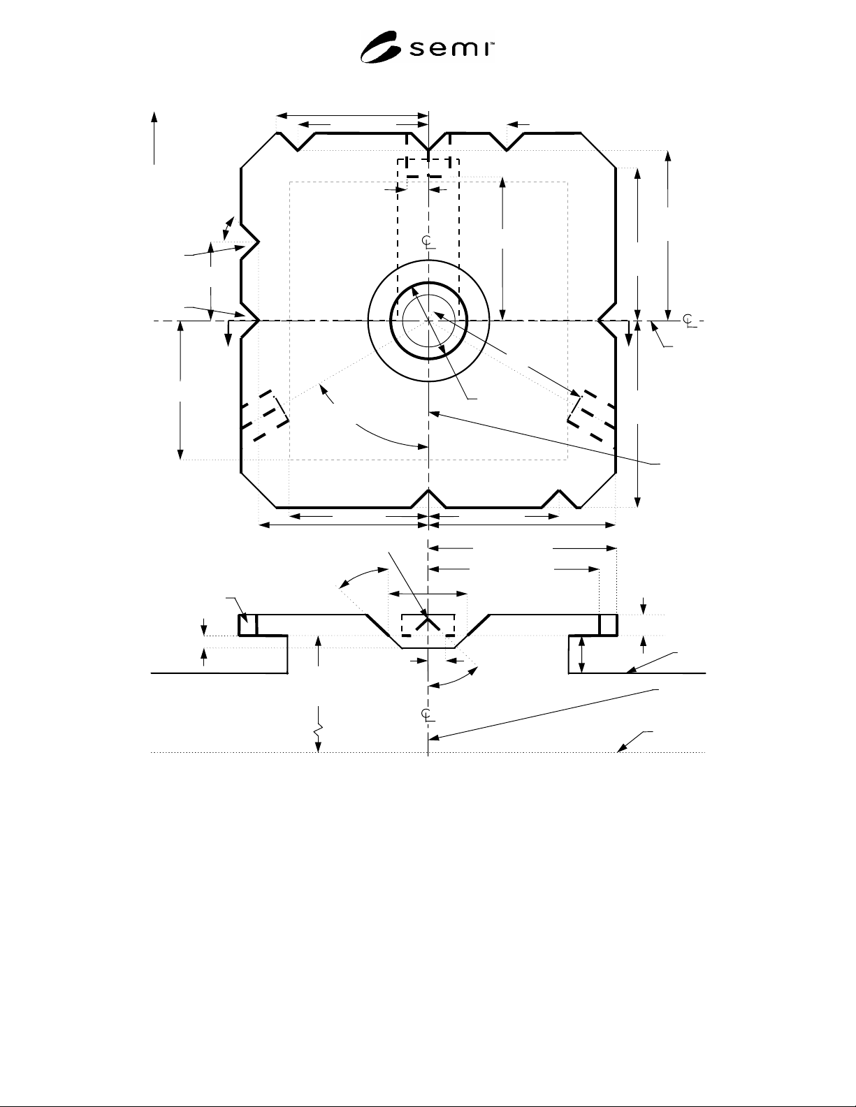
Figure 9
Top Robotic Handling Flange
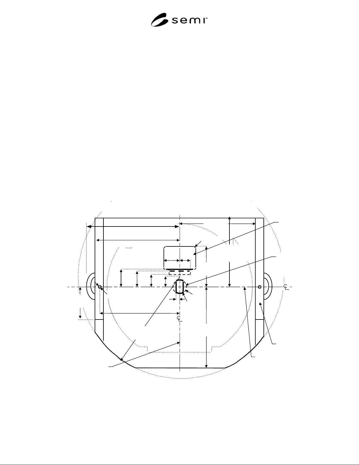
5.11 Retaining Features — Figures 10 and 11 show
two features on the bottom of the FOBIT that may be
used for retaining the FOBIT onto the kinematic
couplings. This may be needed to prevent the FOBIT
from being knocked off the kinematic couplings by the
action of pushing the FOBIT against the front-opening
interface. The front retaining feature contains a ramp
that a wheel might roll up while the FOBIT is being
pushed toward the front-opening interface. The arm
with the wheel (not specified here) then holds the
FOBIT down on the kinematic couplings. The center-
retaining feature consists of an oblong slot with a
chamber above it. The FOBIT can be clamped onto the
kinematic couplings by inserting an oblong head on a
shaft (not specified here) through the slot and rotating it
90° in either direction. Either retaining feature would
only engage after the FOBIT is fully seated on the
kinematic coupling pins. Either retaining feature must
SEMI E119-1104 © SEMI 2002, 2004 12
be able to withstand a force in any direction of at least
f60. It is recommended that SEMI E15.1 tool load ports
be designed to accommodate the minimum hole
dimensions of the retaining features to ensure carrier
interchangeability. Projections on the tool load ports
that mate with the retaining features should also not
interfere with the misalignment correction function of
the kinematic couplings. All dimensions of the FOBIT
(such as the wafer location, etc.) are defined with
reference to the kinematic coupling pins, and are
designed so that all of the their features are in the
proper location only when the FOBIT is held in place
on the kinematic coupling pins by gravity only.
5.12 Sensing Pads and Info Pads — The FOBIT must
have the same carrier sensing pads as defined in SEMI
E1.9, including the info pads that communicate
information about the carrier such as the carrier
capacity (number of wafers) and type (cassette or box).
See SEMI E1.9 for information about info pad
configurations for different wafer carriers similar to
FOBITs including front-opening shipping boxes (as
defined in SEMI M31) and single-wafer interface
(SWIF) systems (as defined in SEMI E103). Two
additional sensing pads (that can be used continuously
while the FOBIT is advancing into the FIMS interface)
must be located near the center of the bottom at the
same distance from the horizontal datum plane as the
carrier sensing pads (See Figure 12). In addition, the
surfaces on the door of the FOBIT that mate with the
seal zones and the reserved spaces for vacuum
application may also be used for door-presence sensing.
It is intended that the FOBIT have the capability to
allow customization of the info pad configuration.
Therefore, the purchaser of 300 mm carriers needs to
specify the desired info pad orientation (up or down)
for all four locations, as defined in the Appendix of
SEMI E1.9.
facial
datum
plane
bottom
conveyor rail
center
retain-
ing
feature
y62
28
x
56 = 194.75 ± 0.25
(at bottom rail)
x
53
195 (elsewhere)
y
52 = 165.5 ± 0.5
(at seal zones, etc.)
166 (elsewhere)
r
60 = 16
± 0.5
r
64
9.5
x
64
35
y
58
75
bilateral
datum
plane
x
57
180
y
53
190
front side of the FOBIT where wafers are accessed
y65
104
x
60
= 8.0 ± 0.5
r
61
16
front
retaining
feature
y67
= 25
r
67
240
y
64
= 42.1
± 0.5
y
63
= 37.3
± 0.5
d
65 =10 ± 0.5
x
65 = 187.5
x
68
25
x50
215 (at human handle)
Figure 10
Bottom View of FOBIT
SEMI E119-1104 © SEMI 2002, 2004 13
z 61
15
z
60
= 8 ± 0.5
y
64 = 42.1 ± 0.5
z62
18
y
62
28
y
65
104
facial
datum plane
horizontal datum plane
of load port
y 63 = 37.3 ± 0.5
= 30
± 0.5°
z63 = 7.5
± 0.5
r 61
16 (above
z 60)
r 60 = 16 ± 0.5 (below
z
60)
front side of the box
where wafers are accessed
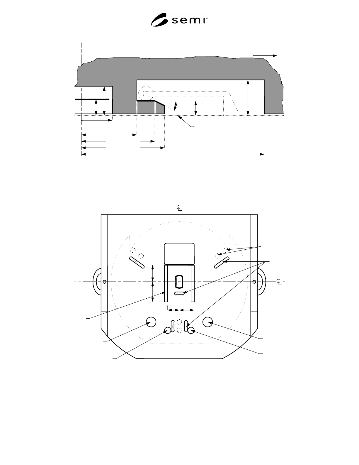
Figure 11
Side View of Retaining Features on Bottom of FOBIT
facial
datum
plane
bilateral
datum
plane
advancing
box
sensing
pads
y64
= 42.1 ± 0.5
y66
50
x
67
34
x
66
31
carrier
sensing
pads
kinematic
pins
info pad D
info pad B
info pad C
info pad A
Figure 12
Sensing Pads on Bottom of FOBIT