semi合集-English.pdf - 第5085页
SEMI M23.2-1000 © SEMI 2000 1 SEMI M23.2-1000 STANDARD FOR ROUND 3 inch (76.2 mm) DIA M ETER POLISHED MONOCRYSTALLINE INDIUM PHOSPHIDE WAFERS This specification was te chnically approved by the Global Com pound Sem icond…
SEMI M23.1-0600 © SEMI 1993, 20001
SEMI M23.1-0600
STANDARD FOR ROUND 50 mm DIAMETER POLISHED
MONOCRYSTALLINE INDIUM PHOSPHIDE WAFERS
This standard was technically approved by the Global Compound Semiconductor Committee and is the direct
responsibility of the Japanese Compound Semiconductor Committee. Current edition approved by the
Japanese Regional Standards Committee on April 28, 2000. Initially available at www.semi.org May 2000;
to be published June 2000. Originally published in 1993; previously published in 1996.
The complete specification for this product includes all general requirements of SEMI M23.
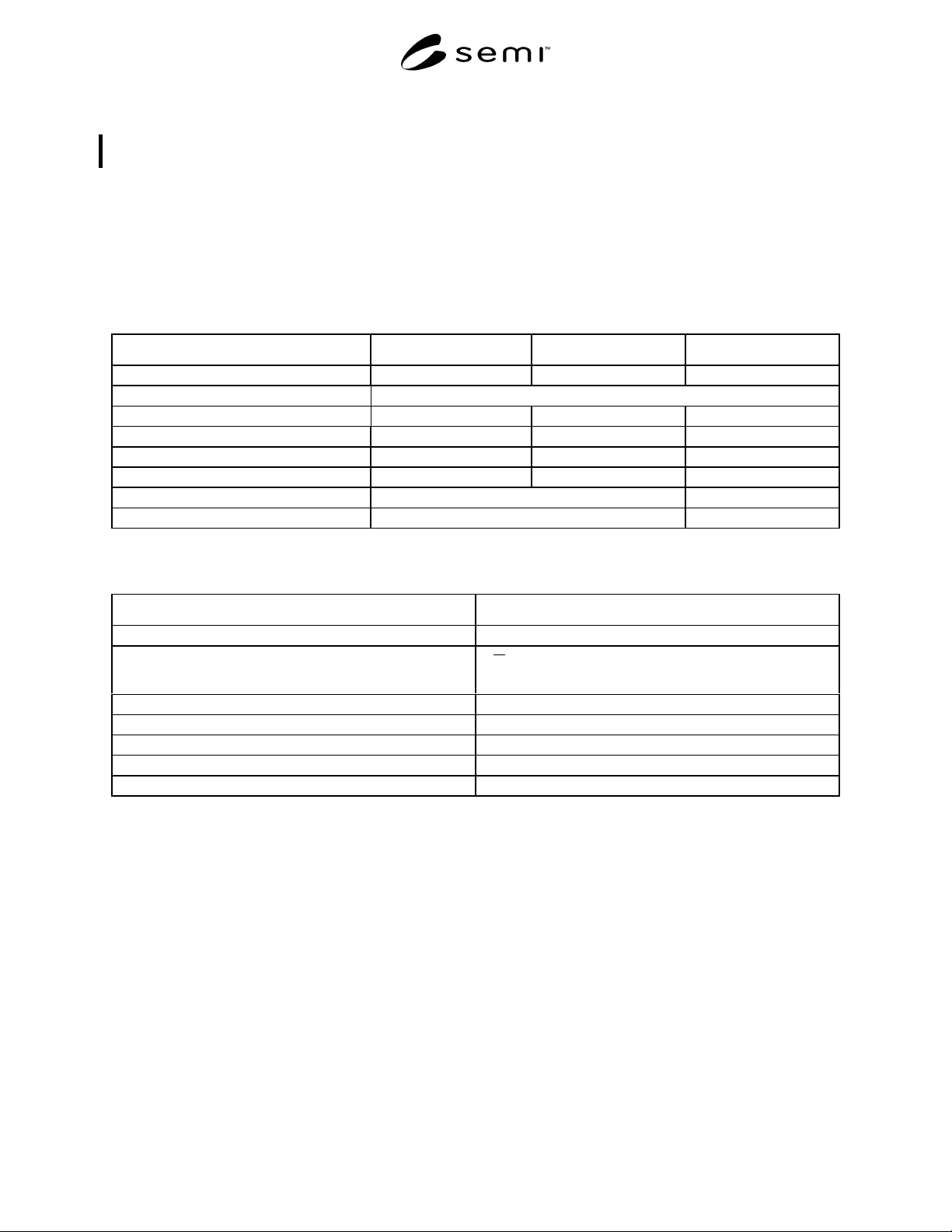
Table 1 Dimension and Tolerance Requirements
Property Dimension Tolerance Units
A
DIAMETER 50.0 ± 0.5 mm
THICKNESS, CENTER POINT
A 350 ± 25 µm
B 450 ± 25 µm
PRIMARY FLAT LENGTH 16 ± 2 mm
SECONDARY FLAT LENGTH 8 ± 2 mm
BOW to be specified
TOTAL THICKNESS VARIATION to be specified
A
: For reference purposes, the metric (SI) units apply.
Table 2 Orientation and Flat Location Requirements
Property Requirement
OPTION Dove-Tail
PRIMARY FLAT ORIENTATION
)110( ± 0.5°, under an indium facet. The primary flat shall be
perpendicular to the “Dove-tail” etch figure.
SECONDARY FLAT ORIENTATION 90 ± 5° clockwise from the primary flat.
SURFACE ORIENTATION
A { 100} ± 0.5°
B { 100} off 2° ± 0.5° toward any { 110} plane
ORTHOGONAL MISORIENTATION ± 5°
NOTICE: SEMI makes no warranties or representations as to the suitability of the standard set forth herein for any
particular application. The determination of the suitability of the standard is solely the responsibility of the user.
Users are cautioned to refer to manufacturer’s instructions, product labels, product data sheets, and other relevant
literature respecting any materials mentioned herein. These standards are subject to change without notice.
The user’s attention is called to the possibility that compliance with this standard may require use of copyrighted
material or of an invention covered by patent rights. By publication of this standard, SEMI takes no position
respecting the validity of any patent rights or copyrights asserted in connection with any item mentioned in this
standard. Users of this standard are expressly advised that determination of any such patent rights or copyrights, and
the risk of infringement of such rights, are entirely their own responsibility.
Copyright by SEMI® (Semiconductor Equipment and Materials
International), 3081 Zanker Road, San Jose, CA 95134. Reproduction o
f
the contents in whole or in part is forbidden without express written
consent of SEMI.
SEMI M23.2-1000 © SEMI 20001
SEMI M23.2-1000
STANDARD FOR ROUND 3 inch (76.2 mm) DIAMETER POLISHED
MONOCRYSTALLINE INDIUM PHOSPHIDE WAFERS
This specification was technically approved by the Global Compound Semiconductor Committee and is the
direct responsibility of the North American Compound Semiconductor Committee. Current edition approved
by the North American Regional Standards Committee on August 28, 2000. Initially available on SEMI
OnLine September 2000; to be published October 2000.
NOTE: The complete specification for this product includes all requirements of SEMI M23.
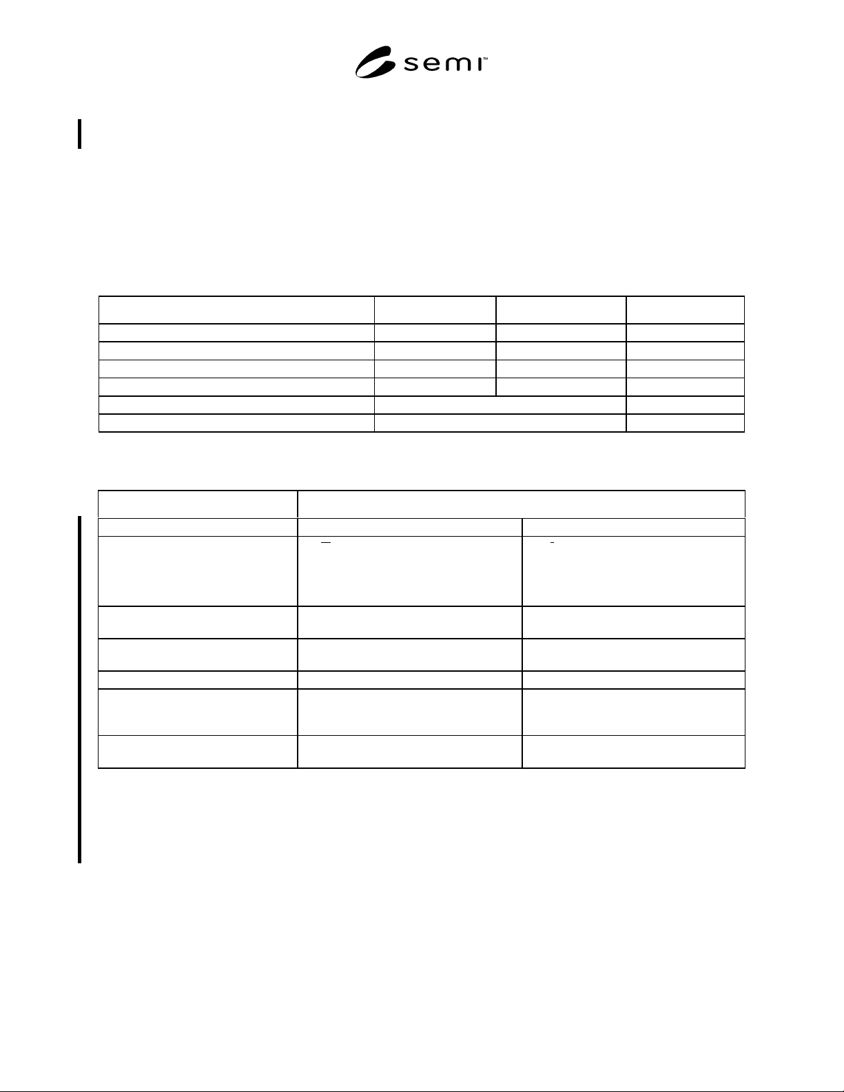
Table 1 Dimension and Tolerance Requirements
Property Dimension Tolerance Units
(See NOTE 1.)
DIAMETER 76.2 ± 0.5 mm
THICKNESS, CENTER POINT 600 ± 25 µm
PRIMARY FLAT LENGTH 22 ± 2 mm
SECONDARY FLAT LENGTH 11 ± 2 mm
BOW to be specified
TOTAL THICKNESS VARIATION to be specified
NOTE 1: For reference purposes, the metric (SI) units apply.
Table 2 Orientation and Flat Location Requirements
Property Requirement
Option Dove-Tail V-Groove
PRIMARY FLAT ORIENTATION
)110( ± 0.5°, (see NOTE 1) under an
indium facet. The primary flat shall be
perpendicular to the “Dove-tail” etch
figure. (See NOTE 2.)
)101( ± 0.5°, (see NOTE 1) under a
phosphorus facet. The primary flat shall
be perpendicular to the “V-Groove” etch
figure. (See NOTE 2.)
SECONDARY FLAT
ORIENTATION
90 ± 5° clockwise from the primary flat. 90 ± 5° counterclockwise from the
primary flat.
SURFACE ORIENTATION (See
NOTE 3.)
A { 100} ± 0.5° (see Figure 1, SEMI M23) { 100} ± 0.5° (see Figure 2, SEMI M23)
B { 100} off 2° ± 0.5° toward any { 110}
plane (see Figure 3)
{ 100} off 2° ± 0.5° toward the { 110}
plane which is between the primary and
secondary flats (see Figure 4)
ORTHOGONAL
MISORIENTATION
± 5° (see Figure 5) ± 5° (see Figure 5)
NOTE 1: See Table 1 in SEMI M23.
NOTE 2: See Figures 1 and 2 in SEMI M23, which show the orientation of the Dovetail and V-groove figures relative to crystallographically
anisotropic pits (see NOTE 4).
NOTE 3: The frame of reference is the (100) plane of the crystal. It is the wafer normal that is tilted towards the (110) plane of the crystal.
NOTE 4: Relating to the etchant used for identifying V-groove and/or dovetail direction, see reference: “HBr-K
2
Cr
2
O
7
- H
2
O etching system for
indium phosphide” J.L.Weyher, et al. Materials Science and Engineering B28 (1994) 488-492.

SEMI M23.2-1000 © SEMI 2000 2
NOTICE: These standards do not purport to address safety issues, if any, associated with their use. It is the
responsibility of the user of these standards to establish appropriate safety and health practices and determine the
applicability of regulatory limitations prior to use. SEMI makes no warranties or representations as to the suitability
of the standards set forth herein for any particular application. The determination of the suitability of the standard is
solely the responsibility of the user. Users are cautioned to refer to manufacturer’s instructions, product labels,
product data sheets, and other relevant literature respecting any materials mentioned herein. These standards are
subject to change without notice.
The user’s attention is called to the possibility that compliance with this standard may require use of copyrighted
material or of an invention covered by patent rights. By publication of this standard, SEMI takes no position
respecting the validity of any patent rights or copyrights asserted in connection with any item mentioned in this
standard. Users of this standard are expressly advised that determination of any such patent rights or copyrights, and
the risk of infringement of such rights, are entirely their own responsibility.
Copyright by SEMI® (Semiconductor Equipment and Materials
International), 3081 Zanker Road, San Jose, CA 95134. Reproduction o
f
the contents in whole or in part is forbidden without express written
consent of SEMI.