semi合集-English.pdf - 第4846页
SEMI M1-0305 © SEMI 1978, 2005 22 6.6 Dimensi onal Characteristics 6.6.1 Dime nsions and Fiducials — The wafers shall conform to the dimen sions, dimensional tolerances, and fiducial (flat or notch) characteristics and l…
SEMI M1-0305 © SEMI 1978, 2005 21
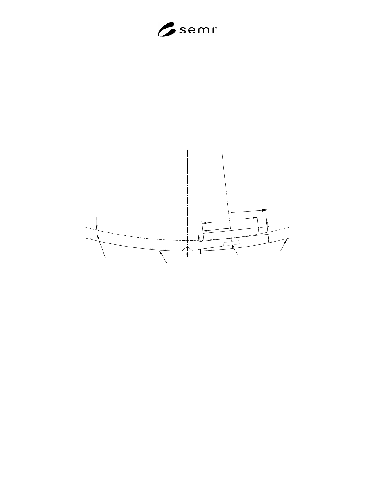
6.5.1.4.2 Single density dot matrix, 5 dots horizontal and 9 dots vertical, shall be used.
6.5.1.4.3 Dot diameter shall be the same as that used for the two-dimensional matrix code symbol (see 6.5.1.4).
6.5.1.4.4 Character dimensions shall be as defined in Table 1 of SEMI M12 (nominal spacing = 1.42 mm, nominal
width = 0.812 mm, nominal height = 1.624 mm).
6.5.1.4.5 Mark location (center of bottommost dot rows) relative to the reference point of the SEMI T7 mark shall
be 1.40 0.05 mm toward the wafer center, as shown in Figure 3.
6.5.1.4.6 Mark field height, as defined by the distance between the centers of the topmost and bottommost dot rows
of the A/N characters, shall be 1.62 0.03 mm (Note 2).
6.5.1.4.7 Mark field length, as defined by the distance between the centers of the leftmost and rightmost dot
columns of the A/N characters, shall be 16.43 0.07 mm.
0
mm
0
5
A
/
N
r
e
a
d
d
i
r
e
c
t
i
o
n
1
6
.
4
3
±
0
.
0
7
5.0° ± 0.1° from
Orientation Fiducial Axis
1
4
8
.
9
5
±
0
.
1
5
f
r
o
m
d
a
t
a
m
a
t
r
i
x
c
o
d
e
s
y
m
b
o
l
r
e
f
e
r
e
n
c
e
p
o
i
n
t
t
o
w
a
f
e
r
c
e
n
t
e
r
All dimensions
in millimeters
unless other-
wise indicated
O
u
t
e
r
P
e
r
i
p
h
e
r
y
o
f
F
Q
A
Edge Exclusion Area
5 mm
Edge Profile Region
Notch
A
/
N
M
AR
K
Orientation Fiducial Axis
[011] ± 1.0°
Wafer Periphery
1
.
6
2
±
0
.
0
3
Wafer Back Surface
8
.
2
2
±
0
.
0
5
Referenc e
Point of SEMI T7 Mark
T
7
M
A
R
K
1
.
4
0
±
0
.
0
5
NOTE: A/N mark field dimensions are defined by the centers of the topmost and bottommost dot rows and
the center of the leftmost and rightmost dot columns of the A/N characters. The field dimensions are more
tightly controlled than those of a field constructed using SEMI M12. This results from the availability of
laser marking capabilities not available when SEMI M12 was developed. In addition, the tolerance on the
field dimensions is not cumulative.
Figure 3
Optional A/N Code Field Location on Back Surface of Notched 300 mm Diameter Wafer (Category 1.15)
NOTE 2: The overall length tolerance of the A/N mark is more stringent than that in SEMI M12. Also the height tolerance of the
overall mark imposes tighter skew and offset tolerances than are required in SEMI M12.
6.5.1.4.8 The mark-field shall be centered on the radius that passes through the reference point of the SEMI T7
mark as shown in Figure 3.
6.5.1.4.9 Character baseline shall be toward wafer OD and parallel with the row of the SEMI T7 mark that contains
that mark’s reference point.
6.5.2 Other — The wafers shall conform to any requirements specified on the purchase order for any other wafer
preparation characteristics including front surface thin films, denuded zone, extrinsic gettering, backseal, annealing,
and edge and back surface conditions.
SEMI M1-0305 © SEMI 1978, 2005 22
6.6 Dimensional Characteristics
6.6.1 Dimensions and Fiducials — The wafers shall conform to the dimensions, dimensional tolerances, and
fiducial (flat or notch) characteristics and locations as specified in the purchase order.
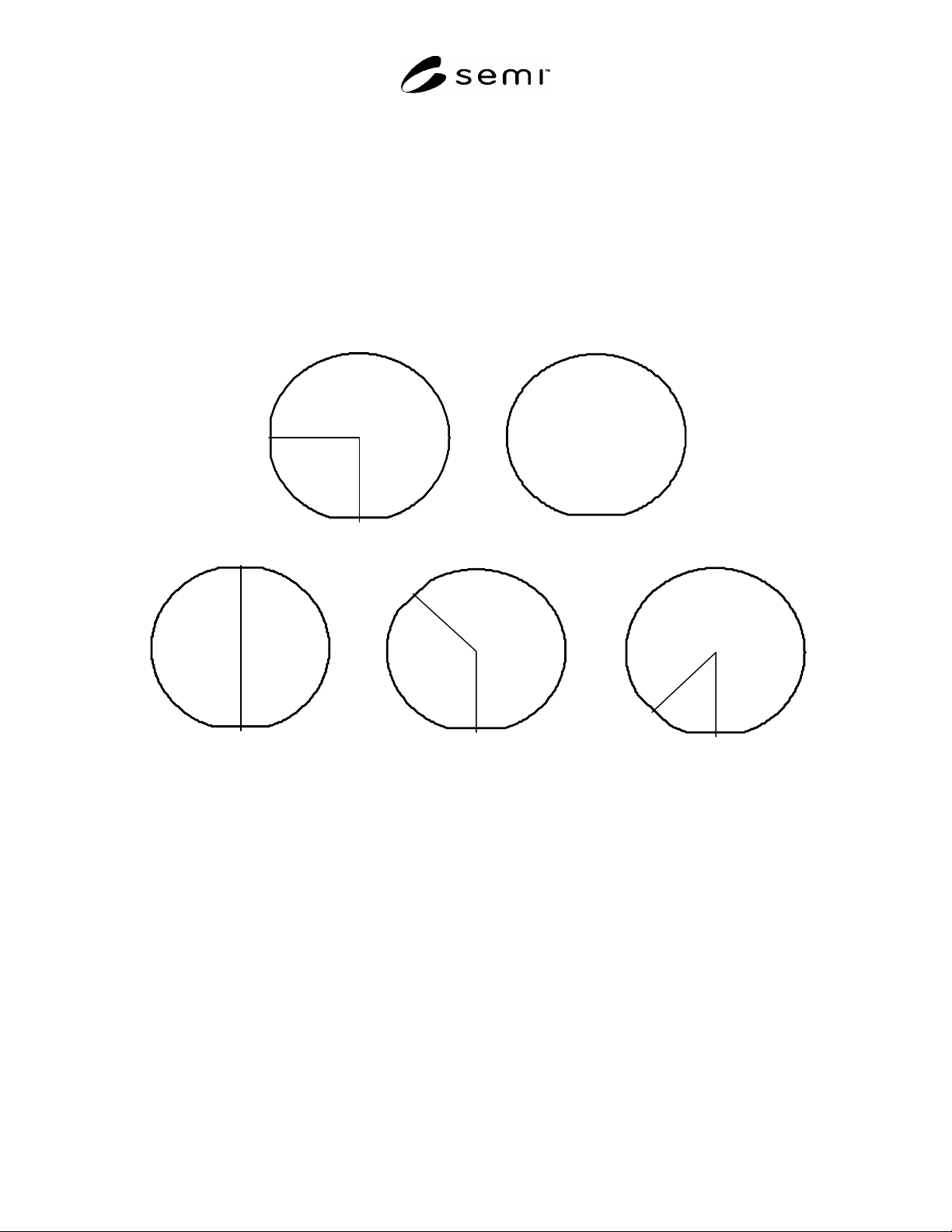
6.6.1.1 Where secondary flats are specified, they shall be located as shown in Figure 4.
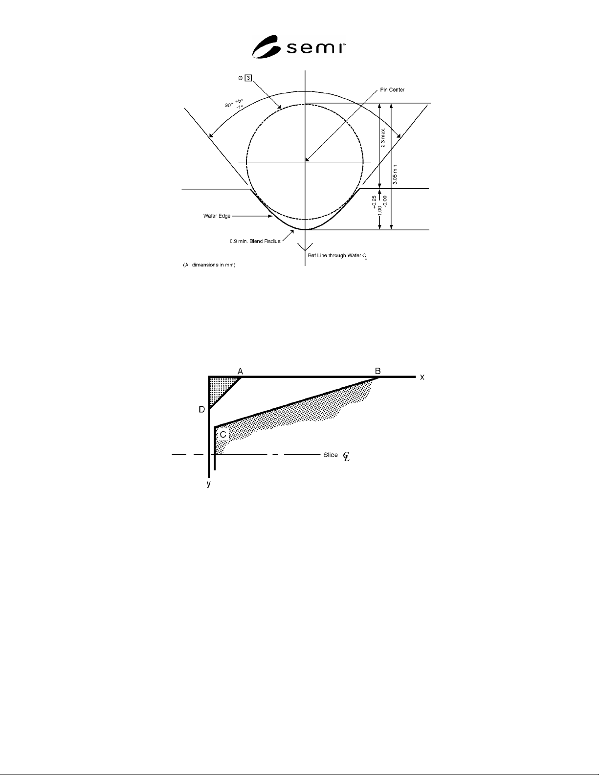
6.6.1.2 Where notches are specified, they shall conform to the dimensions in Figure 5.
6.6.2 Edge Profile — The edge profile of edge-profiled wafers shall conform to the following requirements at all
points on the wafer periphery (except interior portions of notches, if present).
6.6.2.1 The SEMI Wafer Edge Profile Template is shown in Figure 6. There are two sets of dimensions for the
template: T/3 and T/4, where T is the nominal thickness of the wafer (see Tables 4 through 9 for values of the
nominal thickness for various wafer categories).
90
CW
180 CW
135 CW
45 CW
a. (
100) p-type b. (111) p-type
c. (100) n-type d. (100) n-type e. (111) n-type
(wafers 125 mm diameter or less) (150 mm diameter wafers only)
NOTE 1: Secondary flat location for 150 mm diameter (100) n-type wafers changed from configuration c to configuration d
effective January 1, 1990.
NOTE 2: The angular position of the center point of the secondary flat is given in Tables 4 through 6 both in terms of the
clockwise angle from the primary flat, located at the bottom of each figure, to the secondary flat and the angle,
, from the
positive x-axis of the wafer coordinate system as defined by SEMI M20 (at 3 o’clock) to the secondary flat.
Figure 4
Secondary Flat Locations
SEMI M1-0305 © SEMI 1978, 2005 23
NOTE: The pin shown in the outline on this figure is used to align the notched wafer in a fixture during
use. The pin is also used to reference the notched wafer during testing for notch dimensions and
dimensional tolerances. The notch dimensions shown in the figure assume a 3 mm diameter for this
alignment pin.
Figure 5
Notch Dimensions
NOTE 1: The figure is not to scale
NOTE 2: Only one-half of the template is shown; the wafer surface is aligned with the x-axis, and the outermost radial portion of
the edge contour is aligned with the y-axis. The template in this figure is not intended for use in measuring wafer thickness.
NOTE 3: Constant radius profile with blended, tangential front and back surface intercepts is preferred for ease of manufacture
and reduced particle and chip generation.
NOTE 4: The x- and y-axes in this template do not correspond with the x- and y-axes in the wafer coordinate system defined in
SEMI M20.
Figure 6
SEMI Wafer Edge Profile Template