semi合集-English.pdf - 第5374页
SEMI M55-0705 © SEMI 2003, 2004 8 DIN 50445 — Testing of m aterials for semiconduct or technology ; Contactless determinat ion of the elect rical resistivity of semiconductor slices with the eddy current method; Homogene…

SEMI M55-0705 © SEMI 2003, 2004 7
NOTE 11: For microscopic inspection the use of crossed polarisers is recommended. However not all micropipes will be visible
under crossed polarisers.
10.3.4 planar defect — Any anomaly conforming to the definition (see §3) having a maximum width larger than
0.20 mm.
11 Certification
11.1 Upon request of the purchaser in the contract or order, a manufacturer’s or supplier’s certification that the
material was manufactured and tested in accordance with this specification together, with a report of the test results,
shall be furnished at the time of shipment.
11.2 In the interest of controlling inspection costs, the supplier and the purchaser may agree that the material shall
be certified as “capable of meeting” certain requirements. In this context, “capable of meeting” shall signify that the
supplier is not required to perform the appropriate tests in §8. However, if the purchaser performs the test and the
material fails to meet the requirement, the material may be subject to rejection.
12 Packing and Marking
12.1 The wafers supplied under these specifications shall be identified by an individual laser marking consisting of
the supplier assigned lot-number on the backside of each wafer. The laser marking consists of one line of characters
parallel to the primary flat and must be readable with unaided eye. The top of the characters is directed towards the
wafer center. All characters must be completely located within the marking window given in Figure 8. For details
see the appropriate polished Silicon Carbide Wafer Standard.
NOTE 12: SEMI M12 is a standard for the front side marking of silicon wafers and, as a whole, is not applicable to Silicon
Carbide wafers. It is referenced, because some elements of SEMI M12 (see the appropriate polished Silicon Carbide Wafer
Standard) shall also be used for Silicon Carbide.
12.2 Special packing and marking requirements shall be subject to agreement between the supplier and the
purchaser. Otherwise, all wafers shall be handled, inspected, and packed in such a manner as to avoid chipping,
scratches, and contamination in accordance with the best industry practices to provide ample protection against
damage during shipment.
12.3 The wafers shall be identified by appropriately labeling the outside of each box or other container and each
subdivision thereof in which it may reasonably be expected that the wafers will be stored prior to further processing.
Identification shall include as a minimum the nominal diameter, conductive dopant, orientation, resistivity range,
and lot number.
12.4 The lot number, either (1) assigned by the original manufacturer of the wafers, or (2) assigned subsequent to
slice manufacture but providing reference to the original lot number, shall provide easy access to information
concerning the fabrication history of the particular wafers in that lot. Such information shall be retained on file at
the manufacturer's facility for at least 10 years or as negotiated between vendor and user after that particular lot has
been accepted by the purchaser.
13 Related Documents
13.1 ASTM Standards
ASTM F76 Test Methods for Measuring Resistivity and Hall Coefficient and Determining Hall Mobility in
Single-Crystal Semiconductors
ASTM F1241 Terminology of Silicon Technology
13.2 DIN-Standards
DIN 50433/1 — Determination of the Orientation of Single Crystals by Means of X-Ray Diffraction
DIN 50433/3 — Determination of the Orientation of Single Crystals by Means of Laue Back Scattering
DIN 50441/2 — Measurement of the Geometric Dimensions of Semiconductor Wafers: Testing of Edge Profile
DIN 50441/4 — Measurement of the Geometrical Dimensions of Semiconductor Wafers: Slice Diameter, Diameter
Variation, Flat Diameter, Flat Length, Flat Depth
SEMI M55-0705 © SEMI 2003, 2004 8
DIN 50445 — Testing of materials for semiconductor technology; Contactless determination of the electrical
resistivity of semiconductor slices with the eddy current method; Homogeneously doped semiconductor wafers
13.3 ISO Standards
ISO 4287 — Geometrical Product Specifications (GPS) -- Surface texture: Profile method -- Terms, definitions and
surface texture parameters
7
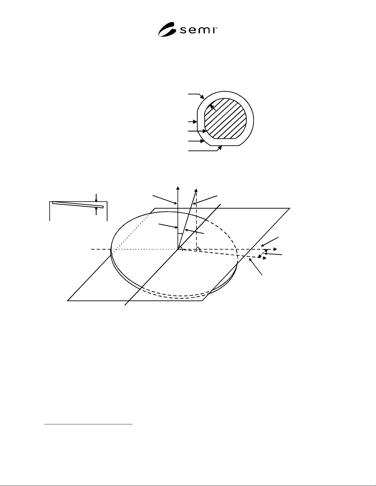
Primary Flat
Secondary Flat
Wafer Periphery
Fixed Quality Area Boundary
X = Nominal Edge Exlusion
Figure 1
Fixed Quality Area
Vector Normal to
Wafer Surface
Orthogonal
Misorientation
Crystallographic c-Axis
<0001>
Tilt Angle
{0001} -Plane
Projection of Wafer Surface Normal
on the {0001} -Plane
Specified Direction of Tilt
(in {0001} -Plane)
Tilt Angle
{0001} Plane
Wafer
Figure 2
Orthogonal Misorientation
7 International Organization for Standardization, ISO Central Secretariat, 1, rue de Varembé, Case postale 56, CH-1211 Geneva 20, Switzerland.
Telephone: 41.22.749.01.11; Fax: 41.22.733.34.30 Website: www.iso.ch
SEMI M55-0705 © SEMI 2003, 2004 9
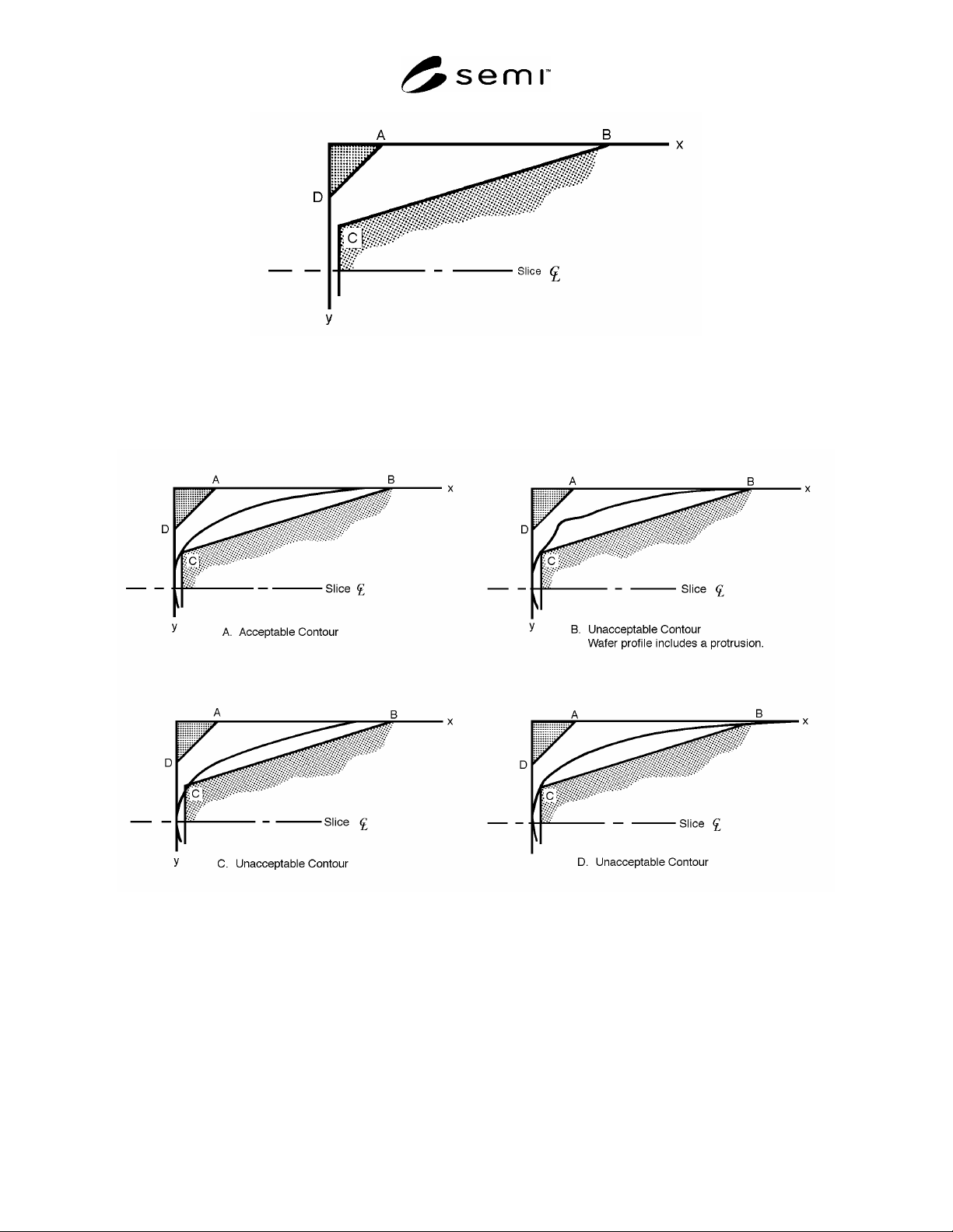
Figure 3
SEMI Wafer Edge Profile Template
NOTE 13: For the exact dimensions and coordinates of points A to D see the appropriate silicon carbide wafer standard.
Figure 4
Examples of Acceptable and Unacceptable Wafer Edge Profiles