semi合集-English.pdf - 第4891页
SEMI M4-1103 © SEMI 1978, 2003 1 SEMI M4-1103 SPECIFICATIONS FOR SOS EPITAXIAL W AFERS This specification was technically approved by th e Global Silicon Wafer Committee and is the direct responsibility of the North Amer…
SEMI M3-0304 © SEMI 1978, 2004 10
RELATED INFORMATION 2
RECOMMENDED SURFACE FINISH CHARACTERISTICS FOR
SAPPHIRE SUBSTRATES
NOTICE: This related information is not an official part of SEMI M3 and was derived from the original edition of
the specifications which erroneously included this optional material as a part of the text of the specification. This
related information was approved for publication by full letter ballot procedure on September 3, 2003.
R2-1 Front Surface Finish
R2-1.1 The substrate should be polished on one side suitable for the epitaxial growth of silicon.
R2-1.2 The quality of this surface may be determined by optical examination at 70× using Nomarski interference
contrast microscopy after etching the substrate in potassium hydroxide at 310°C for one to three minutes.
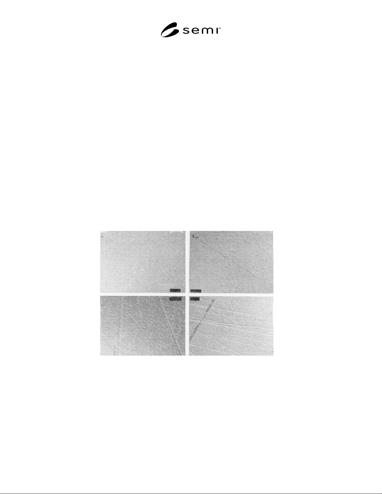
R2-1.3 The photomicrographs in Figures R2-1 through R2-4 may be used as a surface quality guide.
R2-1.3.1 Figure R2-1 shows an acceptable surface.
R2-1.3.2 Figures R2-2 and R2-3 show questionable surfaces that are subject to individual evaluation.
R2-1.3.3 Figure R2-4 shows an unacceptable surface.
R2-2 Back Surface Finish
R2-2.1 The recommended back surface finish is approximately 32 µin, rms, as determined by stylus or optical
profilometer.
Figure R2-1
Acceptable
Surface
Figure R2-3
Questionable
Surface
Figure R2-2
Questionable
Surface
Figure R2-4
Unacceptable
Surface
Figures R2-1 through R2-4
Illustrations of Acceptable, Unacceptable, and Questionable Sapphire Substrate Front Surface Finishes.
NOTICE: SEMI makes no warranties or representations as to the suitability of the standards set forth herein for any
particular application. The determination of the suitability of the standard is solely the responsibility of the user.
Users are cautioned to refer to manufacturer’s instructions, product labels, product data sheets, and other relevant
literature respecting any materials mentioned herein. These standards are subject to change without notice.
The user’s attention is called to the possibility that compliance with this standard may require use of copyrighted
material or of an invention covered by patent rights. By publication of this standard, SEMI takes no position
respecting the validity of any patent rights or copyrights asserted in connection with any item mentioned in this
standard. Users of this standard are expressly advised that determination of any such patent rights or copyrights, and
the risk of infringement of such rights, are entirely their own responsibility.
Copyright by SEMI® (Semiconductor Equipment and Materials
International), 3081 Zanker Road, San Jose, CA 95134. Reproduction o
f
the contents in whole or in part is forbidden without express written
consent of SEMI.

SEMI M4-1103 © SEMI 1978, 2003 1
SEMI M4-1103
SPECIFICATIONS FOR SOS EPITAXIAL WAFERS
This specification was technically approved by the Global Silicon Wafer Committee and is the direct
responsibility of the North American Silicon Wafer Committee. Current edition approved by the North
American Regional Standards Committee on July 27, 2003. Initially available on www.semi.org October
2003; to be published November 2003. Originally published in 1978; previously published July 2003.
1 Purpose
1.1 These specifications cover requirements for
monocrystalline silicon epitaxial layers on sapphire
substrates, used for semiconductor device manufacture.
The combination of a silicon epitaxial layer on a
sapphire substrate is known as a silicon on sapphire
(SOS) epitaxial wafer. By outlining an inspection
process and defining various reject criteria, both
suppliers and purchasers can uniformly define epitaxial
layer quality.
1.2 The defects discussed originate from two sources:
those which are caused by imperfection in the sapphire
substrate and those related to the epitaxial layer,
including handling and packaging.
2 Scope
2.1 The primary standardized properties set forth in
this specification relate to physical, dimensional, and
electrical characteristics of SOS epitaxial wafers.
NOTICE: This standard does not purport to address
safety issues, if any, associated with its use. It is the
responsibility of the users of this standard to establish
appropriate safety and health practices and determine
the applicability of regulatory or other limitations prior
to use.
3 Referenced Standards
3.1 SEMI Standard
SEMI M3 — Specifications for Polished
Monocrystalline Sapphire Substrates
SEMI MF81 — Test Method for Measuring Radial
Resistivity Variation on Silicon Wafers
SEMI MF95 — Test Method for Thickness of Epitaxial
Layers of Silicon on Substrates of the Same Type by
Infrared Reflectance
NOTE 1: Modifications to this procedure are required for use
on SOS wafers.
SEMI MF110 — Test Method for Thickness of
Epitaxial or Diffused Layers in Silicon by the Angle
Lapping and Staining Technique
SEMI MF154 — Guide for Identification of Structures
and Contaminants Seen on Specular Silicon Surfaces
SEMI MF374 — Test Method for Sheet Resistance of
Silicon Epitaxial, Diffused, Polysilicon, and Ion-
implanted Layers Using an In-Line Four-Point Probe
with the Single-Configuration Procedure
SEMI MF523 — Practice for Unaided Visual
Inspection of Polished Silicon Wafers
SEMI MF673 — Test Methods for Measuring
Resistivity of Semiconductor Slices or Sheet Resistance
of Semiconductor Films with a Noncontact Eddy-
Current Gage
3.2 ASTM Standards
1
E 122 — Practice for Choice of Sample Size to
Estimate the Average Quality of a Lot or Process
3.3 Other Standard
2
ANSI/ASQC Z1.4-1993 — Sampling Procedures and
Tables for Inspection by Attributes
NOTICE: Unless otherwise indicated, all documents
cited shall the the latest published versions.
4 Terminology
4.1 Definitions
4.1.1 deposition — the technique involved in the vapor
deposition of single-crystal silicon on oriented sapphire
substrates.
4.1.2 dopant — a chemical element, usually from the
third or fifth columns of the periodic table (typically
phosphorous, arsenic, or boron), incorporated in trace
amounts in the epitaxial layer to establish its
conductivity type and resistivity.
4.1.3 doping — the process of incorporation of a
dopant into the epitaxial layer while the film is
growing.
4.1.4 epitaxial layer — the layer of semiconductor
material that is grown on the substrate.
1 ASTM International, 100 Barr Harbor Drive, West Conshohoken,
PA 19428-2959, USA, Website: www.astm.org, (PracticeE 122 may
be found in Volume 14.02 of the Annual Book of ASTM Standards.)
2 American National Standards Institute, Headquarters: 1819 L
Street, NW, Washington, DC 20036, USA. Telephone: 202.293.8020;
Fax: 202.293.9287, New York Office: 11 West 42nd Street, New
York, NY 10036, USA. Telephone: 212.642.4900; Fax:
212.398.0023, Website: www.ansi.org

SEMI M4-1103 © SEMI 1978, 2003 2
4.1.5 lot — for the purpose of this document, (a) all of
the wafers of nominally identical specification and
characteristics contained in a single shipment, or (b)
subdivisions of large shipments consisting of epitaxial
wafers as above which have been identified by the
supplier as constituting a lot.
4.1.6 pre-epitaxial treatment — the process of etching
an amount of material from the sapphire substrate in
situ prior to deposition.
NOTE 2: Hydrogen (H
2
) gas is commonly used for this
purpose.
4.1.7 resistivity (Ω·cm) — for the purpose of this
method, the volume resistivity, the ratio of the potential
gradient parallel to the current in the material to the
current density.
4.1.8 silicon source — volatile or gaseous silicon
compound.
NOTE 3: Silane (SiH
4
) gas is commonly used for this
purpose.
4.1.9 substrate — the polished sapphire slice upon
which the epitaxial layer is deposited.
4.1.10 surface defects — refers to mechanical
imperfections, SiO
2
residual dust, and other
imperfections visible on the wafer surface. Some
examples of surface defects are: dimples, pits,
particulates, spots, scratches, smears, hillocks, and
polycrystalline regions. Definitions given in SEMI
MF154 shall be used.
4.1.11 wafer, SOS epitaxial — the combined sapphire
substrate with the deposited epitaxial layer.
5 Ordering Information
5.1 Purchase orders for sapphire substrates furnished to
this specification shall refer to SEMI M3.
5.2 Purchase orders for the epitaxial layer on sapphire
substrates furnished to this specification shall include
specifications for the following items:
5.2.1 Silicon source (if required),
5.2.2 Conductivity type and doping source,
5.2.3 Pre-epitaxial treatment (if required),
5.2.4 Thickness and thickness variation,
5.2.5 Resistivity and resistivity variation,
5.2.6 Film crystallinity,
5.2.7 Microparticulate density,
5.2.8 Surface defects and contamination,
5.2.9 Methods of test and measurements (see Section
7),
5.2.10 Lot acceptance procedures (see Section 8),
5.2.11 Certification (if required) (see Section 9), and
5.2.12 Packing and marking (see Section 10).
6 Requirements
6.1 The substrate shall conform to the requirements of
SEMI M3.
6.2 The epitaxial layer shall meet the specification
requirements for the following characteristics as
specified in the purchase order or contract (see Section
5.2).
6.2.1 Pre-epitaxial treatment (if required),
6.2.2 Thickness and thickness variation,
6.2.3 Resistivity and resistivity,
6.2.4 Film crystallinity,
6.2.5 Microparticulate density, and
6.2.6 Surface defects.
6.2.7 Correlation of these characteristics and
verification test procedures or certification of these
characteristics shall be agreed upon between the
supplier and purchaser.
7 Methods of Test and Measurement
7.1 Substrate — Determine by methods agreed upon
between the user and supplier. For measurement
methods, see SEMI M3.
7.2 Epitaxial Layer (See Note 4)
7.2.1 Layer Thickness — Determine by a method
agreed upon between supplier and purchaser. The film
thickness at Point 2, at the wafer center as shown in
Figure 1, is the nominal film thickness for the wafer.
Recommended: SEMI MF95, suitably modified for use
with SOS structures.
7.2.2 Layer Thickness Variation — Unless otherwise
specified, the radial thickness variation shall be
determined from values measured at the center and
edge locations, as shown in Figure 1. Points 1, 3, 4, and
5 are located 6 mm in from the wafer periphery and
define the location of the edge measurements. All
thickness values must be within the specified range. For
example, for a film specified at 0.50 µm ± 10%, all
readings at points 1–5 must be within the range from
0.45 to 0.55 µm.