semi合集-English.pdf - 第4433页
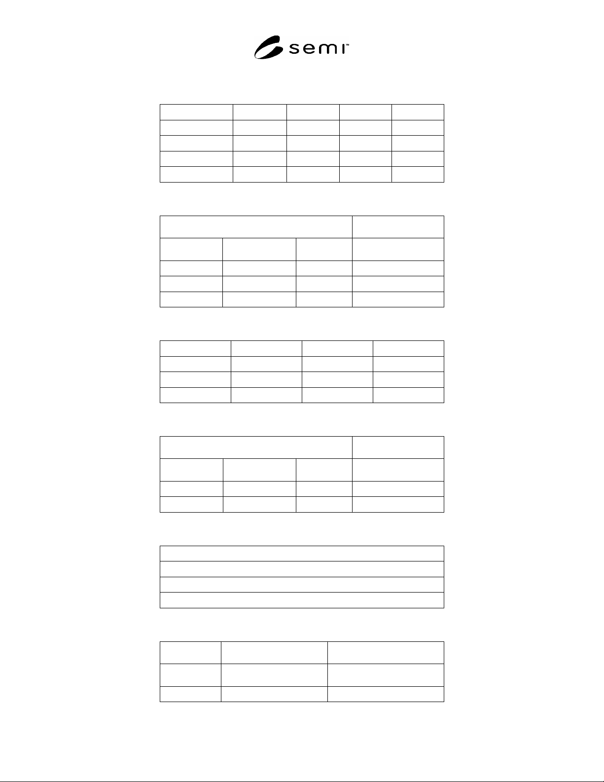
SEMI D6-0305 © SEMI 1992, 2005 2 Table 1 Edge Le ngth (Group A ) in mm 202.8 × 202.8 200 × 250 250 × 250 250 × 300 300 × 300 300 × 350 350 × 350 350 × 400 400 × 400 Table 2 Plate Thickness and Materials (Group A) in mm M…

SEMI D6-0305 © SEMI 1992, 2005 1
SEMI D6-0305
SPECIFICATION FOR LIQUID CRYSTAL DISPLAY (LCD) MASK
SUBSTRATES
This specification was technically approved by the Global Flat Panel Display Mask Committee and is the
direct responsibility of the Japanese Flat Panel Display Materials and Mask. Current edition approved by the
Japanese Regional Standards Committee on January 11, 2005. Initially available at www.semi.org January
2005; to be published March 2005. Originally published in 1992; previously published November 2001.
1 Purpose
1.1 This specification defines standard for substrates used to fabricate liquid crystal display masks.
2 Scope
2.1 This specification applies to photomasks that are principally used in fabricating liquid crystal displays. The edge
lengths specified range from 202.8 × 202.8 mm to 700 × 800 mm.
2.2 Substrates with an edge length less than 200 mm follow the specifications for a semiconductor mask (see
SEMI P1).
NOTICE: This standard does not purport to address safety issues, if any, associated with its use. It is the
responsibility of the users of this standard to establish appropriate safety and health practices and determine the
applicability of regulatory or other limitations prior to use.
3 Referenced Standards
3.1 SEMI Standard
SEMI P1 — Specification for Hard Surface Photomask Substrates
NOTICE: Unless otherwise indicated, all documents cited shall be the latest published versions.
4 Terminology
4.1 None.
5 Ordering Information
5.1 Ordering information shall be discussed between suppliers and users.
6 Edge Length and Thickness Specification
6.1 Edge Length — Units are in mm. See Tables 1 and 2, 3 and 4, 5 and 6, and 7 and 8 for a combination of
materials, edge length, and thickness.
6.2 Edge Length Tolerance — 0.4 mm. Applies to all groups.
6.3 Thickness, Tolerance
6.3.1 Thickness of substrates shall be specified by the edge length group and materials as shown in Tables 2, 4, and
6.
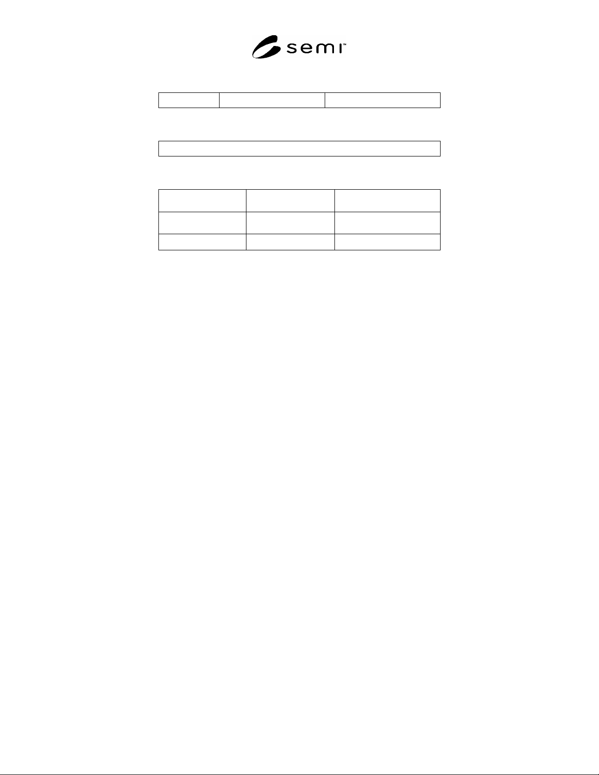
6.3.2 Tolerance — For Groups A and B: –0.4 ~ + 0.2 mm. For Group C: See Table 6. For Group D: See Table 8.
6.4 Material — See §7.
SEMI D6-0305 © SEMI 1992, 2005 2
Table 1 Edge Length (Group A) in mm
202.8 × 202.8
200 × 250 250 × 250
250 × 300 300 × 300
300 × 350 350 × 350
350 × 400 400 × 400
Table 2 Plate Thickness and Materials (Group A) in mm
Material
HTE MTE/LTE ULTE Thickness(mm)
+ + + 3.0
+ 4.8
+ + 5.0
Table 3 Edge Length (Group B) in mm
330 × 450
400 × 500
450 × 550
500 × 600
Table 4 Plate Thickness and Materials (Group B) in mm
Material
HTE MTE/LTE ULTE Thickness(mm)
+ 4.8
+ + 5.0
Table 5 Edge Length (Group C) in mm
620 × 720
650 × 750
650 × 800
700 × 800
Table 6 Plate Thickness and Materials (Group C) in mm
Material
ULTE Thickness (mm) Tolerance (mm)
+ 5.0 ± 0.2
SEMI D6-0305 © SEMI 1992, 2005 3
Table 6 Plate Thickness and Materials (Group C) in mm
+ 8.0 -0.4 ~+ 0.2
Table 7 Edge Length (Group D) in mm
390 × 610
Table 8 Plate Thickness and Materials (Group D) in mm
Material
ULTE Thickness (mm) Tolerance (mm)
+ 6.0
0.2
7 Material Specification
7.1 Substrate material shall be specified as high thermal expansion (HTE), medium thermal expansion (MTE), low
thermal expansion (LTE), or ultra low thermal expansion (ULTE). Examples of HTE materials are soda lime
glasses; of MTE materials are borosilicate and aluminosilicate glasses; of LTE materials are aluminosilicate glasses;
and of ULTE materials are synthetic quartz glasses.
7.2 Substrate materials shall conform to thermal expansion and optical transmittance characteristics specified in
SEMI P1.
7.3 Selected physical properties of HTE, MTE, LTE, and ULTE materials are provided for information in SEMI P1,
Appendix 1.
8 Related Document
8.1 SEMI Standards
SEMI D21 — Terminology for Flat Panel Display Masks
NOTICE: Unless otherwise indicated, all documents cited shall be the latest published versions.
NOTICE: SEMI makes no warranties or representations as to the suitability of the standards set forth herein for any
particular application. The determination of the suitability of the standard is solely the responsibility of the user.
Users are cautioned to refer to manufacturer's instructions, product labels, product data sheets, and other relevant
literature, respecting any materials or equipment mentioned herein. These standards are subject to change without
notice.
By publication of this standard, Semiconductor Equipment and Materials International (SEMI) takes no position
respecting the validity of any patent rights or copyrights asserted in connection with any items mentioned in this
standard. Users of this standard are expressly advised that determination of any such patent rights or copyrights, and
the risk of infringement of such rights are entirely their own responsibility.
Copyright by SEMI® (Semiconductor Equipment and Materials
International), 3081 Zanker Road, San Jose, CA 95134. Reproduction of
the contents in whole or in part is forbidden without express written
consent of SEMI.