semi合集-English.pdf - 第147页
SEMI E19.4-0998 E © SEMI 1992, 2003 3 6.2.5.6 A pod hold-down latc h is require d . The avai lable latch area is specifie d by dimension B1 1 in Figure 2. Latch detail dim ensions are specified in Fig ure 3. 6.2.5.7 The …

SEMI E19.4-0998
E
© SEMI 1992, 2003 2
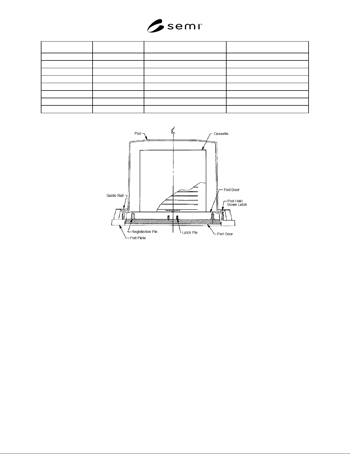
5.2.7 pod door — a removable bottom for the pod that
contains a means for properly positioning the cassette.
5.2.8 pod latch — a mechanical latch that holds the
pod door to the pod until activated by the latch
mechanism pins. Upon activation, the pod door is
released from the pod.
5.2.9 pod latch holes — holes near the center of the
pod door bottom which accept the latch pins.
5.2.10 port assembly — an assembly of the port plate
and port door that includes the guide rails, registration
pins, latch pins, and pod hold-down latches.
5.2.11 port door — a door for the port plate opening
that provides a mating surface for the bottom of the pod
door when the pod is in place on the port plate. The port
door contains the registration pins and the pod door
latch pins.
5.2.12 port plate — a horizontal mating surface for the
base of the pod that provides a seal surface for the
bottom surface of the pod perimeter. The port plate
contains the guide rails and the pod hold-down latches.
5.2.13 registration holes — holes in the bottom of the
pod door that fit over registration pins in the top of the
port door when the pod is placed on the port door.
5.2.14 registration pins — pins that provide fixed
position and orientation between the port door and pod
door and assist in the final positioning of the pod on the
port assembly. The registration pins fit into the
registration holes in the bottom of the pod door.
6 Requirements
NOTE 2: The requirements and dimensions for the design of
mechanical interface standard ports and pods are given in this
section. See Table 1 for 200 mm (8 inch) Port Dimensions.
6.1 Cassette Sizes — All specifications are related to
200 mm wafers held in an appropriate cassette. It is
understood that smaller diameter wafers and other
substrates may be contained in pods which are
compatible with this standard.
6.2 Port Design Requirements — The general design
of the port is shown in Figures 2 and 3. Design
requirements for the interface components are provided
in Sections 6.2.1 through 6.2.5.
6.2.1 Port Door — Dimensions A1 through A3 specify
the port door top view. The gap between port door and
port plate is not specified, but should be kept to a
minimum distance to restrict particle movement.
6.2.2 Pod Guide — The inside distance of the corner
guides of the port is specified by B1 and B2. The length
of the corner is specified by B12. The corner guides
may be connected by guide rails if desired.
6.2.3 Latch Pins — Two latch pins are located around
the port door center. For location of the pins, see C1,
C2, and C3.
6.2.4 Registration Pins — The three registration pins
on the port door are located asymmetrically, and spaced
by dimensions D1 through D4. The size of the pins is
specified by D5 through D7.
6.2.5 Pod — The bottom surfaces of the pod body and
pod door shall conform to the specified port
dimensions. The upper part of the pod body and top
surface of the pod door must fit and hold in place the
cassette for 200 mm (8 inch) wafers. Although the pod
dimensions are not explicitly specified by this standard,
the following requirements apply:
6.2.5.1 The bottom surfaces of the pod door at its
perimeter shall match the dimensions of the port door
top (A1 through A3). The tolerances shall be chosen so
that the pod door does not extend over the port door in
any instance, even when the port door is built to its
minimal acceptable dimensions and potential variance
between registration pins and holes is considered. This
is to ensure an interference-free passage of the pod door
through the port opening.
6.2.5.2 The base of the pod body shall fit freely but
with close tolerance between the guide rails (B1, B2,
and B9), which not only hold the pod in place while the
port is open, but also provide proper alignment for
closure of the pod at the end of the open/shut cycle.
6.2.5.3 The bottom surface of the pod requires three
registration holes to engage with the registration pins on
the port. The registration pins shall be positioned in the
door bottom so that the registration pins prevent seating
of the pod with the port in the event that the pod is
improperly rotated by 180 degrees from the correct
orientation. The correct orientation is illustrated in
Figure 2.
6.2.5.4 The perimeter of the bottom surface of the pod
body shall be continuous and shall be positioned against
the port surface. This positioning assures the activation
of an optional limit switch, placed in an unspecified
location along the port perimeter, for the sensing of
proper pod placement.
6.2.5.5 The center of the cassette crossbar shall
coincide with the center of the pod door, with the
cassette oriented as shown in Figure 2. The top surface
of the pod door requires the registration bars that hold
the cassette in place. The horizontal cassette movement
is limited by the tolerances G2. The vertical position of
the cassette while located on the pod door is specified
by the distance G1 between the top of the port surface
and the bottom surface of the cassette.
SEMI E19.4-0998
E
© SEMI 1992, 2003 3
6.2.5.6 A pod hold-down latch is required. The available latch area is specified by dimension B11 in Figure 2. Latch
detail dimensions are specified in Figure 3.
6.2.5.7 The pod latch holes have a dimension of I1 perpendicular to the plane connecting both holes.
6.2.5.8 Positions for latches are identified in Figure 2 by positions 1, 2, 3, and 4. The following options for hold-
down latch positions are defined by this specification:
Option A Positions 1 and 2
Option B Positions 3 and 4
Option C Positions 1, 2, 3, and 4
7 References
The following articles describe the standard mechanical interface concept:
“The Challenge to Control Contamination: A Novel Technique for the IC Process,” The Journal of Environmental
Sciences (May/June 1984), page 23.
“SMIF, A Technology for Wafer Cassette Transfer in VLSI Manufacturing,” Solid State Technology (July 1984),
page 111.
The complete specification for this interface includes all general requirements of SEMI E19.
Table 1 Port Dimensions for 200 mm (8 inch) Wafer Cassette
Feature Dimension Label Metric English
Port Door A1 135.84 mm ± 0.13 mm (5.348 in. ± 0.005 in.)
A2 131.06 mm ± 0.13 mm (5.160 in. ± 0.005 in.)
A3 13.08 mm ± 0.25 mm (0.515 in. radius ± 0.010 in.)
A4 0.38 mm ± 0.13 mm (0.015 in. ± 0.005 in.)
Guide Rails B1 146.48 mm ± 0.13 mm (5.767 in. ± 0.005 in.)
B2 141.71 mm ± 0.13 mm (5.579 in. ± 0.005 in.)
B3
B4
B5 29.97 mm maximum (1.18 in. maximum)
B6
B7 16 mm minimum (0.630 in. minimum)
B8 45° maximum (45° maximum)
B9 22.22 mm radius maximum (0.875 in. radius maximum)
B10
B11 50.8 mm maximum (2.00 in. maximum)
B12 26.9 mm minimum (1.06 in. minimum)
Latch Pins C1 16° ± 0° 30' (16° ± 0° 30' )
C2 86° ± 0° 30' (86° ± 0° 30' )
C3 26.72 mm ± 0.05 mm (1.052 in. diameter ± 0.002 in.)
C4 3.175 mm ± 0.025 mm (0.125 in. diameter ± 0.001 in.)
C5
C6 9.14 mm ± 0.25 mm (0.360 in. ± 0.010 in.)
C7 Full Spherical Radius Full Spherical Radius
C8
Registration Pins D1 183.39 mm ± 0.25 mm (7.22 in. ± 0.010 in.)
D2 91.69 mm ± 0.13 mm (3.610 in. ± 0.005 in.)
D3 231.78 mm ± 0.25 mm (9.125 in. ± 0.010 in.)
D4 116.59 mm ± 0.13 mm (4.590 in. ± 0.005 in.)
SEMI E19.4-0998
E
© SEMI 1992, 2003 4
Feature Dimension Label Metric English
D5 6.35 mm ± 0.025 mm (0.250 in. diameter ± 0.001 in.)
D6 16.26 mm ± 0.25 mm (0.640 in. ± 0.010 in.)
D7 Full Spherical Radius Full Spherical Radius
Latch Pin F1 0.8 Nm minimum (7 in. lbf. minimum)
Force (Torque) 1.7 Nm maximum (15 in. lbf. maximum)
Position of Cassette G1 20.70 mm ± 0.25 mm (0.815 in. ± 0.010 in.)
G2 H-Bar Centered ± 0.51 mm (H-Bar Centered ± 0.020 in.)
Pod Latch Holes I1 3.4 mm ± 0.1 mm (0.135 in. ± 0.004 in.)
Figure 1
Port Terminology