semi合集-English.pdf - 第5146页
SEMI M31-0705 © SEMI 1998, 2005 6 5.9 Internal Vertical Dimensions — Figures 3 through 7 show the vertical dim ensions of the internal F OSB. Note that z 8 (the height of the bottom nom inal wafer seating plane above the…
SEMI M31-0705 © SEMI 1998, 2005 5
are turned more than 45° toward the position that unlocks the automated door from the box, the latch key holes on
the door must be such that the door is not removable from the latch keys. There are no door seal zone requirements
for the manual door option, but a FOSB with the manual door must contain a frame seal zone that meets the frame
seal zone requirements specified in this section.
5.6 Wafer Retaining — When the FOSB is closed, the wafers must be retained in the FOSB to prevent movement
during subsequent handling, including shipping. It should be noted that wafers are typically shipped in a vertical
orientation and generally require support from a secondary package. It is recommended that this secondary package
be designed to allow for easy removal of the FOSB from the secondary package.
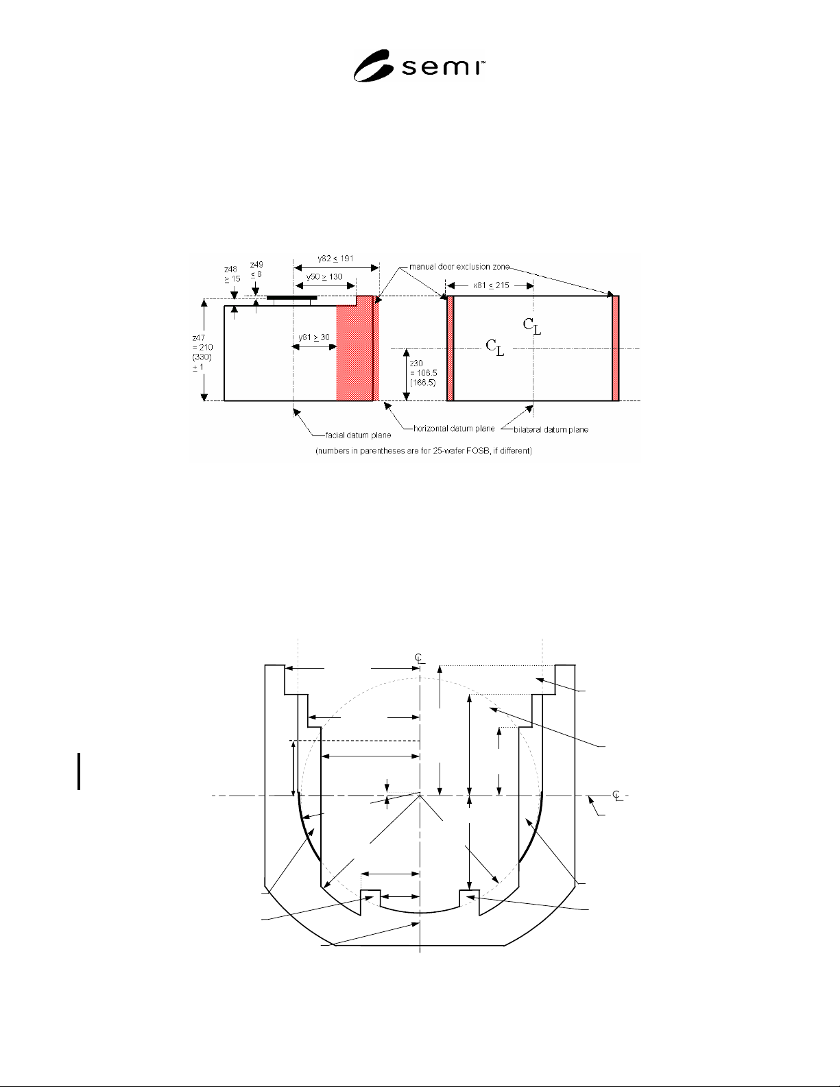
Figure 1
Manual Door Area
5.7 Wafer Orientation and Numbering — The wafers must be horizontal when the FOSB is placed on the coupling,
and the wafers slots are numbered in increasing order from bottom to top (so the bottom wafer is wafer number 1,
the next wafer up is wafer number 2, etc.).
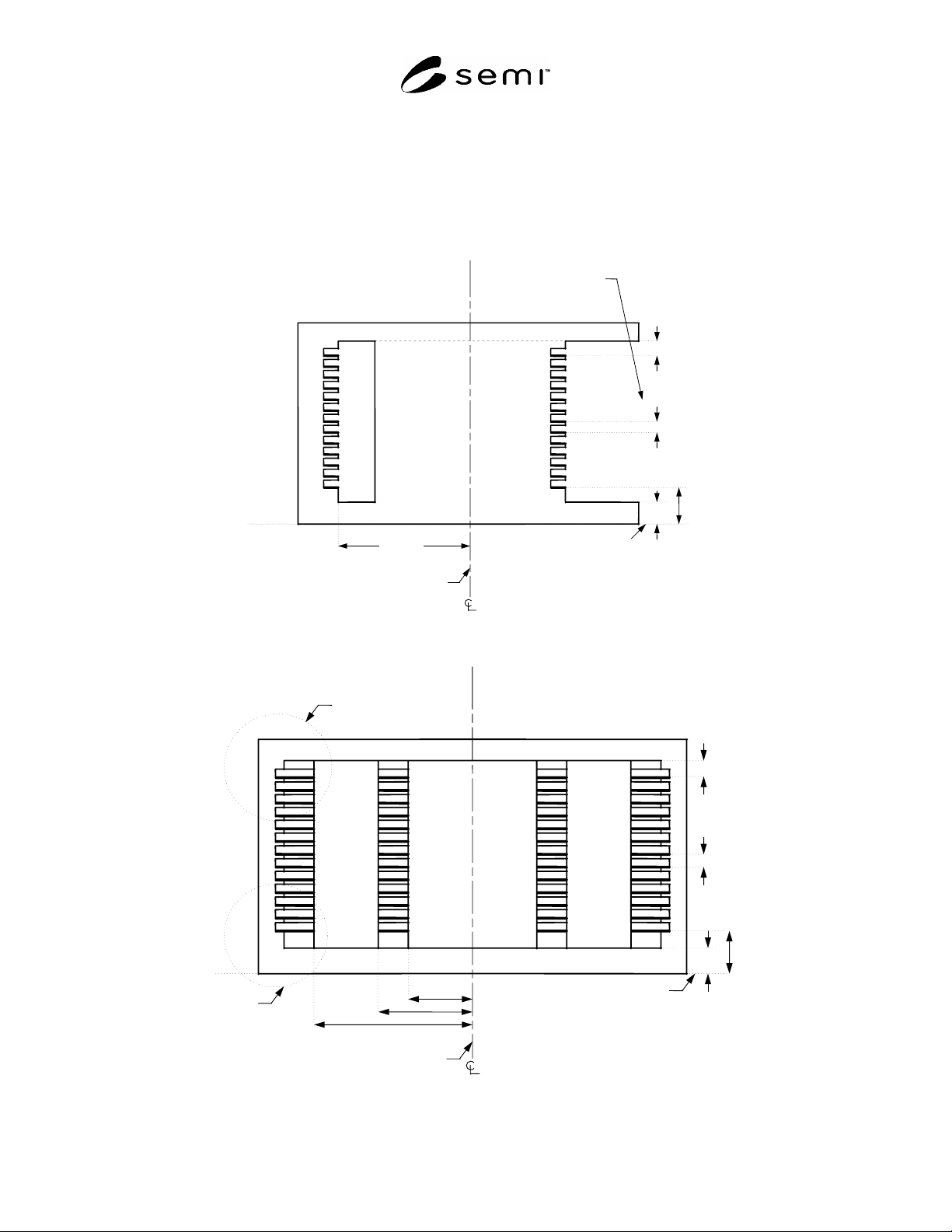
5.8 Internal Horizontal Dimensions — Figure 2 shows a cross-section of the horizontal boundaries of the FOSB
side domains (which contain the parts of the FOSB higher than z6 above the horizontal datum plane and lower than
z15 above the top wafer). In this and following figures, the most heavy lines are used for surfaces that have
tolerances (not surfaces that have only maximum or minimum dimensions).
y 5
120
y
52
165.5 ±
0.5 mm
(6.52 ±
0.02 in.)
y 49
134
y 11
85
x
52
170
facial
datum
p
lane
x
51
140
x
3
125
x
1
50
x
2
75
bilateral
datum
p
lane
r 4
170
ri
g
ht rea
r
side domain
left rea
r
side domain
front side of the FOSB where wafers are accessed
left front
side domain
wafer
p
ick-u
p
area
ri
g
ht front
side domain
r 1
151
r 2 =152
r 3
r 2 + 1
wafer set-
down and
extraction
volumes
y
1
3
+1
–
0
y51
50(manual door)
140(automated
door)
Figure 2
Top View of FOSB Internal Dimensions
SEMI M31-0705 © SEMI 1998, 2005 6
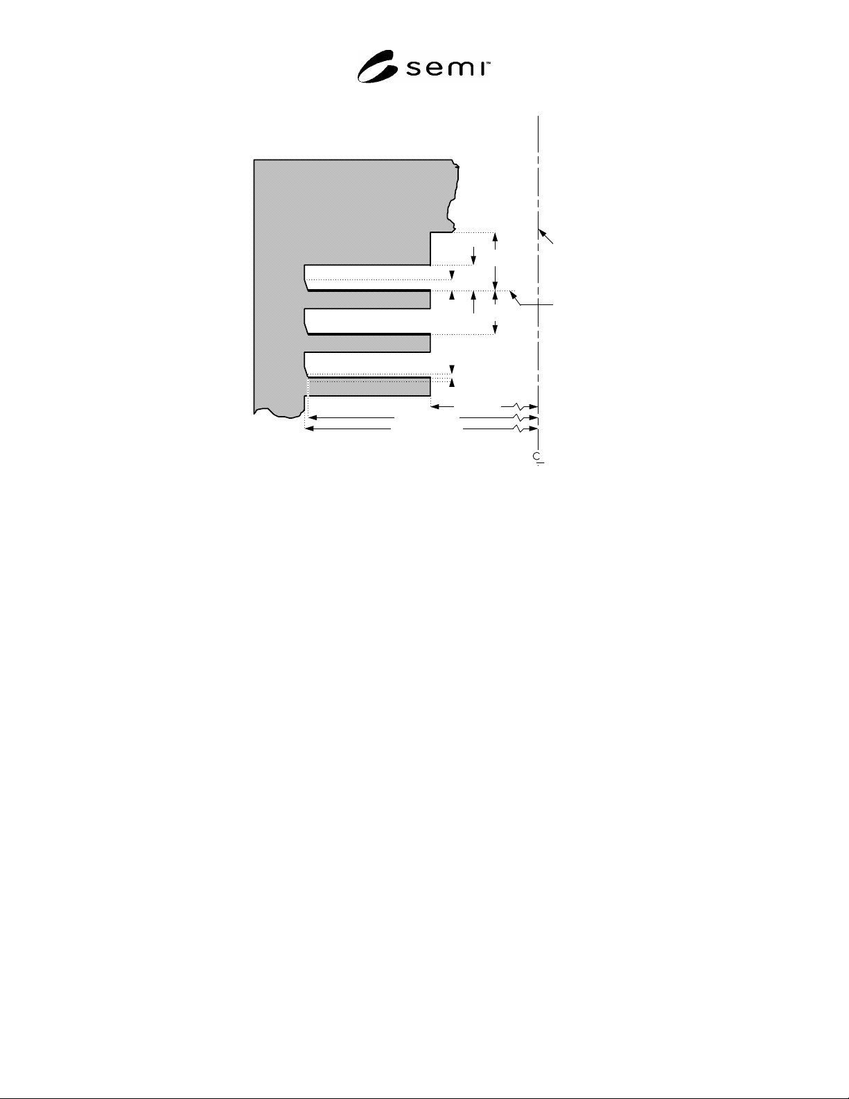
5.9 Internal Vertical Dimensions — Figures 3 through 7 show the vertical dimensions of the internal FOSB. Note
that z8 (the height of the bottom nominal wafer seating plane above the horizontal datum plane) and z12 (the
distance between adjacent nominal wafer seating planes) are given as absolute distances with no tolerance. This
means that the sum of actual height variations in the FOSB from the kinematic coupling to the supporting features
holding each wafer must be contained within the tolerance of z10 with no further stack-up at each higher wafer. The
method for meeting this requirement is left up to the FOSB supplier. Table 2 defines all dimensions for Figures 3
through 7.
Figure 3
Side View of FOSB Internal Dimensions
Figure 4
Front View of FOSB Internal Dimensions
horizontal
datum
plane
z
8
= 44
z
15
13
z
6
32
z
12
= 10
y
5
120
facial datum plane
front side of the FOSB where wafers
are accessed
detail in
Figure 8
detail in
Figure 6
horizontal datum plane
z
8
= 44
z
15
13
z
6
32
x
1
50
x2
75
x3
125
z
12
= 10
bilateral datum plane
SEMI M31-0705 © SEMI 1998, 2005 7
z15 13
z11
6
z12 =10
x3 125
bilateral
datum
plane
z23 3
top
nominal
wafer
plane
z10 =±0.5
(height of
wafer bottom)
r2 =152
r3 r2 + 1
+1
–0
Figure 5
Upper Cross-Section at Facial Datum Plane
5.9.1 Wafer Set-Down Volume — The open space for the wafer set-down volume consists of a cylindrical section
with radius r2 and a main axis parallel to and y1 in front of the nominal wafer centerline. The top of this cylindrical
section is z11 above the nominal wafer seating plane and its bottom is z10 above the nominal wafer seating plane.
The implications for wafer positioning of the tolerance on r2 are as follows. The wafers should be placed in the
FOSB within a circle of radius corresponding to the smaller bound on r2 to avoid touching the edge of the wafer to
the side of the FOSB. Once the wafer has been placed, the FOSB must not allow a wafer to move outside of a circle
of radius corresponding to the larger bound on r2. There are two exceptions to this limit on wafer movement. When
the wafer is pushed toward the rear of the FOSB, the location of the wafer is defined by the wafer pick-up volume
(see ¶5.9.3). When the FOSB is gently tilted forward up to 45°, the wafers may slide forward, but it is recommended
that they not extend further than y20 from the facial datum plane. This may be accomplished by designing the teeth
supporting the wafers to include a “wafer stopper” at the front that is outside of r2 and under z29 as illustrated in
Figure 6.
5.9.2 Wafer Extraction Volume — The open space for the wafer extraction volume includes a cylindrical section
with radius r3 and a main axis parallel to and y1 in front of the nominal wafer center line. The top of this cylindrical
section is z11 above the nominal wafer seating plane and its bottom is z23 above the nominal wafer seating plane.
The wafer extraction volume also includes the extrusion out the front of the FOSB of this cylindrical section and the
portion of the wafer set-down volume above z29. The implications for wafer extraction of the definition of
dimension r3 (r3 r2 + 1) are as follows. The FOSB must give an extra 1 mm (0.04 in.) of horizontal clearance
once the wafer is picked up from wherever it ends up (within the bounds of r2) after transport in the FOSB.