semi合集-English.pdf - 第44页
SEMI E2-93 © SEMI 1986, 2003 2 4 Referenced Documents SEMI M1 — Specifications for Polished Monocrystalline Silicon Wafers SEMI M3 — Specifications for Polished Mono- crystalline Sapphire Substrates SEMI M9 — Specificati…
SEMI E2-93 © SEMI 1986, 2003 1
SEMI E2-93 (Withdrawn 1103)
SPECIFICATIONS FOR QUARTZ AND HIGH TEMPERATURE WAFER
CARRIERS
These specifications were technically reapproved by the Physical Interfaces & Carriers Committee and are
the direct responsibility of the North American Physical Interfaces & Carriers Committee. Current edition
approved by the North American Regional Standards Committee in October 1998. Initially available at
www.semi.org February 1999; to be published February 1999. Originally published in 1986; previous
published revision in 1996.
NOTICE: This document was balloted and approved
for withdrawal in 2003.
1 Scope
1.1 These specifications cover the dimensional
requirements for quartz and high temperature wafer
carriers used in processing wafers. These general
requirements assist in the compatibility of wafer
carriers and most automated wafer processing
equipment. Wafer pre-orientation is recommended
before transferring wafers into quartz carriers to avoid
interference between the flat fiducial(s) and carrier
slots. These standards are intended to promote the
interchangeability of wafer carriers and encourage the
production of equipment suitable to a greater
percentage of the market.
1.2 The design definitions of SEMI Wafer Carrier
Specifications assume compliance to wafer dimensions
defined in SEMI M1, M3, or M9. For a wafer carrier to
be said to “meet the SEMI specifications,” it must be
manufactured within the dimensional limits of the given
specification, and in addition be dimensionally stable
within specification when used in accordance with
manufacturer' s recommendations. Since wafer carriers
are manufactured from a number of different raw
materials and several different manufacturing methods,
it is up to each manufacturer to determine the
recommended usage for each wafer carrier type. The
specifications were not established nor do they
represent or suggest a means to obtain any ideal
efficiencies in wafer processing results or quality of end
product.
1.3 For referee purposes, SI (System International,
commonly called metric) units shall be used for 80 mm
and larger diameter wafers.
2 Selected Definitions
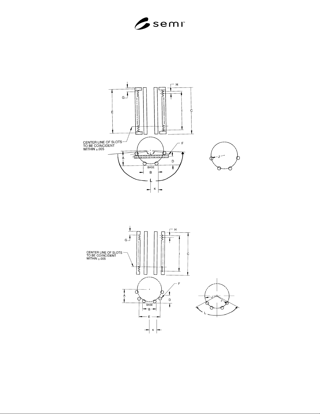
2.1 For illustrations of terms, see Figure 1 for Carrier
Style 1, and Figure 2 for Carrier Style 2. Dimensions
and tolerances are given in Table 1 of the standards for
carriers of the appropriate wafer diameter.
2.1.1 base — the material at the bottom of the carrier
that the carrier rests on when placed on a flat reference
surface.
2.1.2 bottom plane — a horizontal plane tangent to the
base.
2.1.3 end — either end of carrier parallel to wafer
plane.
2.1.4 lift access — the clearance space used to insert an
implement to pick up a wafer carrier.
2.1.5 side — either one of the sides perpendicular to
the wafer plane.
3 Dimension Definitions
Symbol
A
Wafer Height — distance from the horizontal center line
of the wafer to the bottom plane
B
Base Width — the outside dimension of the base from
side to side
C Base Length — length of the base from end to end
D
Lift Access Height — distance from horizontal
centerline of lift access opening to bottom plane
E
Lift Access Spacing — distance from center line to
center line of lift access opening
F
Lift Access Opening — size of opening for the insertion
of an implement to pick up the carrier
G
Base End to First Slot — the distance from either end of
the carrier to the first slot on same end
H
Slot Spacing — the distance from the center line of one
slot to the center line of the adjacent slot
I
End Slot to other End Slot — the center line of the first
slot on either end to the center line of the slot on the
other end
J
Pocket Size — the diameter of a circle coincident to the
bottom of all wafer slots in a wafer position
K
Base Side to Wafer Center line — horizontal distance
from the vertical wafer center line to either side of the
base
L
Carrier Region — region enclosed by the greatest
included angle between a line drawn from the center
point of the wafer and the outermost member of the
carrier on one side and a similar line on the other side
P Separation — separation of wafers when placed in slots
SEMI E2-93 © SEMI 1986, 2003 2
4 Referenced Documents
SEMI M1 — Specifications for Polished
Monocrystalline Silicon Wafers
SEMI M3 — Specifications for Polished Mono-
crystalline Sapphire Substrates
SEMI M9 — Specifications for Polished Mono-
crystalline Gallium Arsenide Slices
Figure 1
Style 1: Non-Contiguous 25 & 50 Slot
Figure 2
Style 2: Contiguous 25 & 50 Slot
SEMI E2-93 © SEMI 1986, 2003 3
APPLICATION NOTE
NOTE: The material contained in these application notes is not an official part of SEMI E2 and is not meant to modify or
supersede it in any way. Rather, these notes are provided primarly as a source of information to aid in the application of the
standard, as such, they are to be considered as reference material only. The standard should be referred to in all cases.
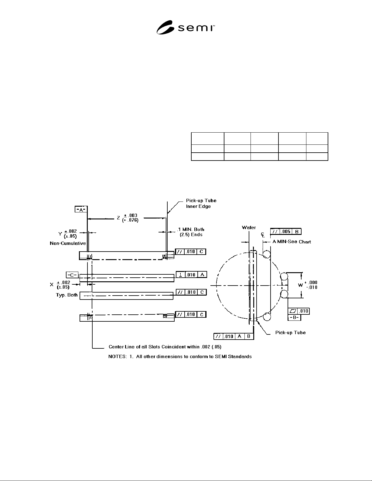
Table A1-1 lists the dimensions in linear, versus
angular, measurements for ease of dimensional
verification. The dimensions fall within SEMI
specification; however, they correspond closer to an
“L” angular dimension of 140 degrees versus the 150
degrees. The figures A1-1 and A1-2 illustrate these
dimensions for non-contiguous and contiguous style
quartz carriers.
A1-1 Carrier — Dimension L
Automated mass transfer of silicon wafers requires
edge contact below the centerline of the wafer
according to Table 1. These dimensions have been
determined as the minimum distance below the wafer
center line allowing the gripping mechanism to overlap
the vertical tangent of the wafer edge below the
centerline. This overlap allows the wafers to be
passively crattled. Contacting the wafer any higher
toward the centerline will require clamping force on the
wafers.
Table A1-1
Wafer Size 100 mm 125 mm 150 mm 200 mm
A 18 mm 21 mm 25 mm 32 mm
Style I & II (0.70" ) (0.82" ) (1.00" ) (1.25" )
Figure A1-1
Style 1: Non-Contiguous