semi合集-English.pdf - 第5277页
SEMI M46-1101 E © SEMI 2001 3 7.3 Instru mentatio n 7.3.1 Capacitance M eter — C apable of m easurin g valu es up to 300 nF, em ploying a test sig nal of amplitu de less than 100 mV R MS. The measu r em ent frequen cy sh…

SEMI M46-1101
E
© SEMI 2001 2
5.1.2 A rectifying barrier, of known contact area, is
formed by placing the sample in contact with an
electrolyte.
5.1.3 The quality of the barrier is assessed using I-V
and C-V measurements.
5.1.4 From the measured C-V data the carrier
concentration of the layer is determined.
5.1.5 The sample is anodically etched to produce a new
barrier deeper in the material. The etch depth is
determined using Faraday’s law of electrolysis.
5.1.6 Sections 5.1.4 and 5.1.5 are repeated to generate
a carrier concentration vs. depth profile.
6 Interferences
6.1 Thin Layers — Diffusion of carriers into adjacent
regions set a fundamental resolution limit to the
measurement. In addition if the layer has a high sheet
resistivity this can also affect the value obtained.
6.2 Double Layer Capacitance — A limitation
imposed by the physical nature of the
electrolyte/semiconductor barrier which sets an upper
limit to the measured carrier concentration, for accurate
measurements, of 1 × 10
19
cm
-3
. The technique can be
used beyond this value, but with progressive
degradation.
6.3 Etch Well Uniformity
6.3.1 Etch Well Flatness — Non-uniformity increases
the effective area and may result in the measurement
not being wholly made in the layer of interest. The
main causes of non-uniformity are gas bubbles,
inadequate electrolyte circulation and uneven
illumination.
6.3.2 Etch Well Roughness — indicates poor etching
and has a deleterious effect on the measurements.
Generally overcome by selecting a more appropriate
electrolyte and/or etching conditions.
6.4 Non-Ideal Electrical Characteristics
6.4.1 Series Resistance — From the contacts, sample
and electrolyte affect the accuracy of the measurements.
This effect is minimized by using a highly conductive
electrolyte, making large area ohmic contacts and by
employing a low measurement frequency.
6.4.2 Leakage Currents — Parallel conduction can
affect the accuracy of the measurement. Its influence is
reduced by employing a high measurement frequency.
6.4.3 Large Excess Area — Can give rise to errors on
n-type material particularly when profiling Hi-Lo
structures. The excess area is electrolyte dependent but
is mainly affected by the quality of the seal used to
define the area. Large excess areas indicate a poor seal
and are corrected by replacing the seal.
6.5 Hi-Lo Structures — Measurement is subject to
inaccuracy due to carrier diffusion and excess area
errors. For accurate measurements, chemically etch to
the layer of interest before measurement.
6.6 Contact Quality — Non-Ohmic or high resistance
contacts have a deleterious effect on the measurement.
Contacts should be checked by measuring the resistance
between two similar contacts and then reversing the
current direction and repeating the measurement.
6.7 Surface and Deep States — Cause the measured
capacitance to be frequency dependent and/or
dependent on the rate at which the bias is changed.
Usually resolved by using a high measurement
frequency. This should not be confused with the
frequency dependence which is more usually attributed
to high series resistance.
6.8 Surface Films — Have a deleterious effect on the
capacitance measurement. Film formation should be
avoided by using an appropriate electrolyte, control of
the etching bias and time and by electrolyte circulation.
6.9 Surface Roughness — The surface of the sample
should be smooth and free of features that would affect
the action of the seal.
6.10 Light — Light can affect the capacitance
measurement, so the sample must be placed in a dark
environment during the measurement.
6.11 Sample Loading — The accuracy of the
measurement depends on the repeatability of the area. If
a compliant seal is involved, such as a plastic ring, the
sample should be held in contact with the seal by
applying a controlled and constant force. No relative
lateral movement should take place during the loading
process.
6.12 Ring Variability — The condition of the ring has a
large effect on the measurement. Good seals will have a
small to zero excess area and exhibit a well defined and
reproducible contact area.
7 Apparatus
7.1 Measurement of Etch Well and Ring Areas —
Measuring microscope with either an XY stage, with a
linear resolution of 0.01 mm or better, or a camera and
image processing system capable of measuring an area
of 0.1 cm
2
to better than 0.5%.
7.2 Measurement of Etch Well Flatness — (Optional)
A means such as a stylus profiler for checking the
flatness and roughness of the etch well. In most cases
visual inspection of the etch well, for a mirror like
appearance, is sufficient indication of low roughness.
SEMI M46-1101
E
© SEMI 2001 3
7.3 Instrumentation
7.3.1 Capacitance Meter — Capable of measuring
values up to 300 nF, employing a test signal of
amplitude less than 100 mV RMS. The measurement
frequency should be typically between 1 and 100 kHz.
7.3.2 Equivalent Circuit Model — The meter should
assume a parallel circuit model for the
electrolyte/semiconductor interface and provision
should be made to compensate for the large series
resistance of the electrolyte and contacts.
7.3.3 Potentiostat — Capable of maintaining the
potential of the sample with respect to a reference
electrode constant to ±5mV during the measurement
and with a reference input impedance of > 10
13
Ohms.
7.3.4 Light Source — A source of uniform illumination
of above band gap energy for etching n-type materials.
7.4 Sample Holder
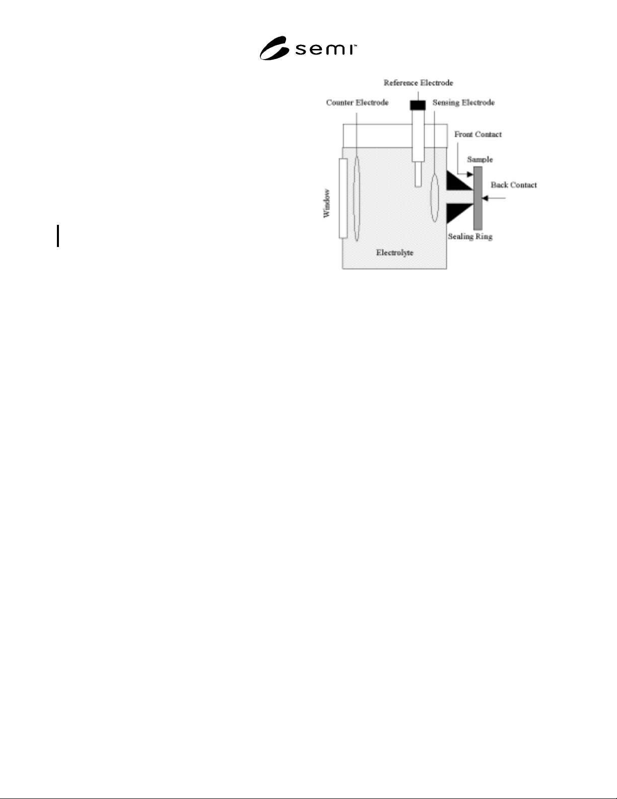
7.4.1 Electrochemical Cell — Used to hold the sample,
contain the electrolyte and support the sealing ring and
other electrodes, see Figure 1.
7.4.1.1 Sealing Ring — A corrosion resistant ring
which forms a seal between the electrolyte and the
sample. This ring defines the measurement area which
should be reproducible and well defined. The ring area
should not be less than 0.008 cm
2
and the
reproducibility between runs should be better than ±
3%. Large ring areas (typically ≥ 0.1 cm
2
) are preferred
for more accurate measurements.
7.4.1.2 Reference Electrode — Used to control the
sample bias via a potentiostat.
7.4.1.3 Counter Electrode — The bias and test signals
are applied between this electrode and the sample.
Figure 1
Electrochemical Cell
7.4.1.4 Sensing Electrode — Placed close to the
sample-electrolyte interface and used to measure the
admittance of the sample.
7.4.1.5 Sample Contacts — Ohmic contacts to the front
and/or back surface of the sample for the purpose of
applying bias.
8 Reagents and Materials
8.1 Purity of Reagents — All chemicals for which such
specifications exist shall conform to SEMI C1.
8.2 Purity of Water — Use either distilled or de-
ionized water having a resistivity greater than
2 MOhm•cm at 25
o
C as determined by the Non-Referee
Test of Test Methods D 1125.
8.3 Selection of Electrolyte — The choice of
electrolyte is not defined by this standard and is up to
the discretion of the user or by agreement between the
customer and the supplier.
8.3.1 InP, GaAs and Related Compounds — Preferred
electrolyte, Na
2
.EDTA (0.1 M) basified with
ethylenediamine to a pH of 10, although other
electrolytes can be satisfactorily used.
NOTE 1: Preferred electrolyte, see reference
“Electrochemical C-V Profiling of Heterojunction Device
Structures” A.C.Seabaugh et al. IEEE Trans on Electron Dev
36 No 2 (1989) 309-313.
9 Safety Precautions
9.1 The electrolytes used are potentially hazardous.
Read the Materials Safety Data Sheets before
attempting to prepare the electrolytes. Use safety

SEMI M46-1101
E
© SEMI 2001 4
eyewear, rubber gloves and protective clothing. Prepare
all electrolytes in a fume hood.
9.2 Ensure that all electrolytes are correctly labeled.
10 Specimen Preparation
10.1 The sample should be free from surface debris
and scratches. The sample should be cleaned with
deionized (DI) water and dried.
10.2 To measure a single layer or upper layer of a
multilayered structure, no additional sample preparation
is required.
10.3 For a buried layer in a multilayered structure,
measurement accuracy is improved by removing the
overlaying layers by either the use of selective or
controlled chemical etches.
10.4 If the upper layers cannot be removed by
chemical etching then the sample can be profiled
electrochemically but in some cases this may reduce the
accuracy of the method.
10.5 For conducting substrates Ohmic contacts should
be made to either the front or back of the wafer. For
insulating substrates an Ohmic contact should be made
to the front of the epilayer. Contacts are formed
electrically, by alloying or by any other suitable
method. The quality of the contact should be verified
electrically.
11 Calibration and Standardization
11.1 Sealing Ring — Calibration of the sealing ring
areas is performed using a “blue slice”, made by
growing an anodic oxide film on a polished n-type
substrate.
11.1.1 The “blue slice” is profiled according to this test
method. Etch only the minimum amount necessary to
see the illuminated area (typically 0.5 µm). Flush the
cell several times with DI water before removing the
sample. Wash and measure the sample as soon as
possible.
11.1.2 Wetted Area — The wetted area is observed due
to chemical attack of the oxide film and is measured
using a measuring microscope with cross hair eye-
pieces and micrometer XY stage or by using a zoom
camera and image processing system.
11.1.3 Illuminated Area — Etches in the light and
forms a well defined etch well, which is measured as
per the wetted area.
11.1.4 Calibration Interval — Regularly check the area
and condition of the sealing ring. For daily use, the ring
areas should be calibrated at least three times a week.
11.1.5 Replacement — Rings should be replaced if the
excess area exceeds 10% for rings of area ≤ 0.05 cm
2
or
5% for rings of area > 0.05 cm
2
or if the perimeter is
not uniform.
11.1.6 Alternative Calibration Method — The areas
can be measured using known n and p-type test
samples. This method is best suited for continual
monitoring of the ring area between “blue slice”
calibrations.
11.2 Instrumentation — The bias voltage,
measurement frequency and capacitance measurement
should be checked annually.
11.2.1 Bias — The bias voltage should be checked
with a DVM with an input impedance > 1 MOhm.
11.2.2 Capacitance — The capacitance measurement
should be checked using calibrated fixed value
capacitors covering the expected sample capacitance
range or from 1–100 nF.
11.2.3 Frequency — The measurement frequency
should be checked with a frequency counter.
12 Measurement Procedure
12.1 Choice of Electrolyte — An electrolyte should be
selected that forms a rectifying barrier with the sample,
gives a flat, mirror finish etch well and generates only a
small excess area.
12.2 Sample Mounting — A region of the sample
should be defined which will form the rectifying
contact with the electrolyte. This area can be defined by
some form of sealing ring or mask, but it is important
that the area of contact between the electrolyte and the
sample be precisely known and remain constant during
the measurement.
12.2.1 Sealing Ring — If the sample is pressed against
a sealing ring, the seal must be cleaned with DI water
and dried before positioning the sample. If the sample
needs repositioning, the sample and sealing ring should
be recleaned and dried.
12.2.2 Ring Loading — As the mounting pressure may
effect the reproducibility of the measurement and the
lifetime of the sealing ring, it must be controlled (e.g.
by the reproducible use of a suitable compression
spring).
12.3 Cell Filling and Debubbling — Fill the cell,
which holds the sealing ring and other measurement
electrodes, with the electrolyte. The process of filling
the cell frequently traps bubbles of air on the surface of
the sample. These bubbles must be removed before a
measurement can be made.