semi合集-English.pdf - 第7867页
SEMI T13-1104 © SEMI 2004 27 List 1 An Example of D evice Tracking Data in XML <? xml version ="1.0" encoding ="utf-8" ?> < DeviceTrackingData xmlns ="urn:semi-org:xsd.Doc3754.V0312.Devi…
SEMI T13-1104 © SEMI 2004 26
RELATED INFORMATION 1
DEVICE TRACKING EXAMPLES
NOTICE: This related information is not an official part of SEMI T13 and was derived from the Japanese
Traceability Committee. This related information was approved for publication by full letter ballot on April 30,
2004.
R1-1 Device Tracking Report
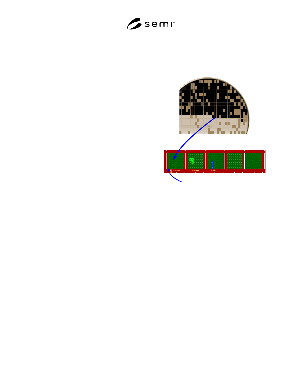
R1-1.1 The following figurer and list are example of
Device Tracking Report.
R1-1.1.1 Device Example — The following Figure
shows a device picked from a wafer and placed on a
strip.
R1-1.1.2 Report Example — The following list shows
an example of the report for the first 2 devices on a strip
taken from Wafer1 and the next 2 taken from Wafer2.
From Substrate
OriginLocation(0,0) = "LowerLeftTop"
RowColumnMajor = "Column"
FromX
FromY
To Substrate
Index = 15
Rows = 6
Columns = 40
ToX = 2
ToY = 4
Figure R1-1
SEMI T13-1104 © SEMI 2004 27
List 1 An Example of Device Tracking Data in XML
<?xml version="1.0" encoding="utf-8" ?>
<
DeviceTrackingData xmlns="urn:semi-org:xsd.Doc3754.V0312.DeviceTrackingData">
<SubstrateType>Strip</SubstrateType>
<SubstrateId>MyStrip</SubstrateId>
<LayoutId>Device</LayoutId>
<OriginLocation>LowerLeftTop</OriginLocation>
<RowColumnMajor>Column</RowColumnMajor>
<FromSubstrate>
<SubstrateType>Wafer</SubstrateType>
<SubstrateId>Wafer1</SubstrateId>
<D><X>10</X><Y>18</Y></D>
<D><X>7</
X><Y>17</Y></D>
</FromSubstrate>
<FromSubstrate>
<SubstrateType>Wafer</SubstrateType>
<SubstrateId>Wafer2</SubstrateId>
<D><X>18</X><Y>1</Y></D>
<D><X>9</X><Y>0</Y></D>
</FromSubstrate>
</
DeviceTrackingData>
NOTE 1: The <D> elements contain the X and Y location on the substrate from which they came.
NOTE 2: The <FromSubstrate> element specifies the substrate type and identifier from which the devices came from.
NOTE 3: The <D> elements represent each device on the layout “Device” for strip “MyStrip”.
NOTE 4: The number of <D> entries must equal Rows * Columns defined in the “Device” layout.
NOTE 5: The one dimensional array of <D> elements represents the two dimensional array of locations defined in the “Devices” layout in
RowColumnMajor format with respect to the OriginLocation.
NOTE 6: The OriginLocation corresponds to the definition of the same name in SEMI G81.
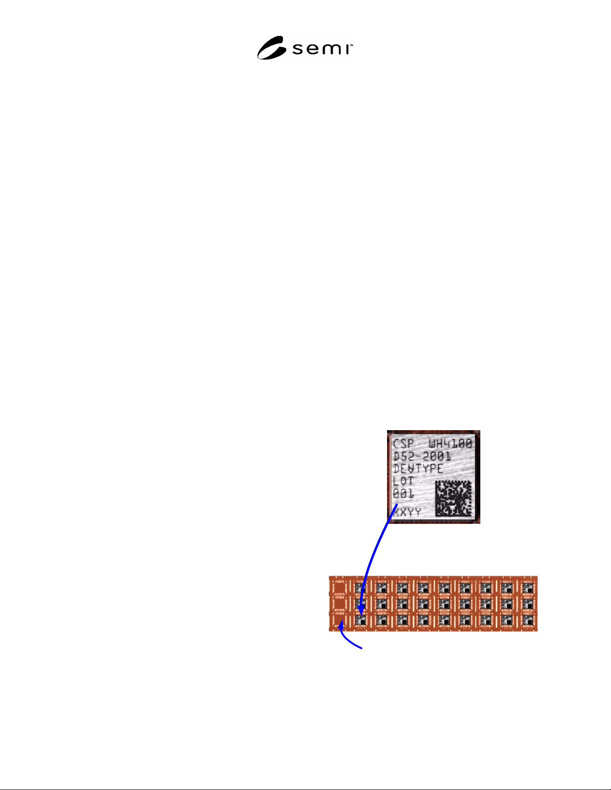
R1-2 Device ID Report
R1-2.1 ID Example — The following figure shows a
strip of devices with alphanumeric and 2D matrix
marks. The unique part of the 2D mark is “LOT001-
XXYY”.
R1-2.2 Report Example — The following list shows a
truncated version of the Device Id Data report for the
strip shown in upper figure.
Substrate
Index = 3
Rows = 3
Columns = 10
ToX = 1
ToY = 1
OriginLocation (0,0) ="LowerLeftTop"
RowColumnMajor="Column"
DeviceId
Figure R1-2
SEMI T13-1104 © SEMI 2004 28
List 2 An Example of Device ID Data in XML
<?xml version="1.0" encoding="utf-8" ?>
<
DeviceIdData xmlns="urn:semi-org:xsd.Doc3754.V0312.DeviceIdData">
<SubstrateType>Strip</SubstrateType>
<SubstrateId>MyStrip</SubstrateId>
<LayoutId>Device</LayoutId>
<OriginLocation>LowerLeftTop</OriginLocation>
<RowColumnMajor>Column</RowColumnMajor>
<D><Id></Id></D>
<D><Id></Id></D>
<D><Id></Id></D>
<D><Id>Lot001-XXYY</Id></D>
<D><
Id>etc.</Id></D>
</
DeviceIdData>
NOTE 1:The <D> elements contain a tracking code marked on the package that is unique for the manufacturer and product.
NOTE 2: The <D> elements represent each device on the layout “Device” for strip “MyStrip”.
NOTE 3: The number of <D> entries must equal Rows * Columns defined in the “Device” layout.
NOTE 4: The one dimensional array of <D> elements represents the two dimensional array of locations defined in the “Devices” layout in
RowColumnMajor format with respect to the OriginLocation.
NOTE 5: The OriginLocation corresponds to the definition of the same name in SEMI G81.
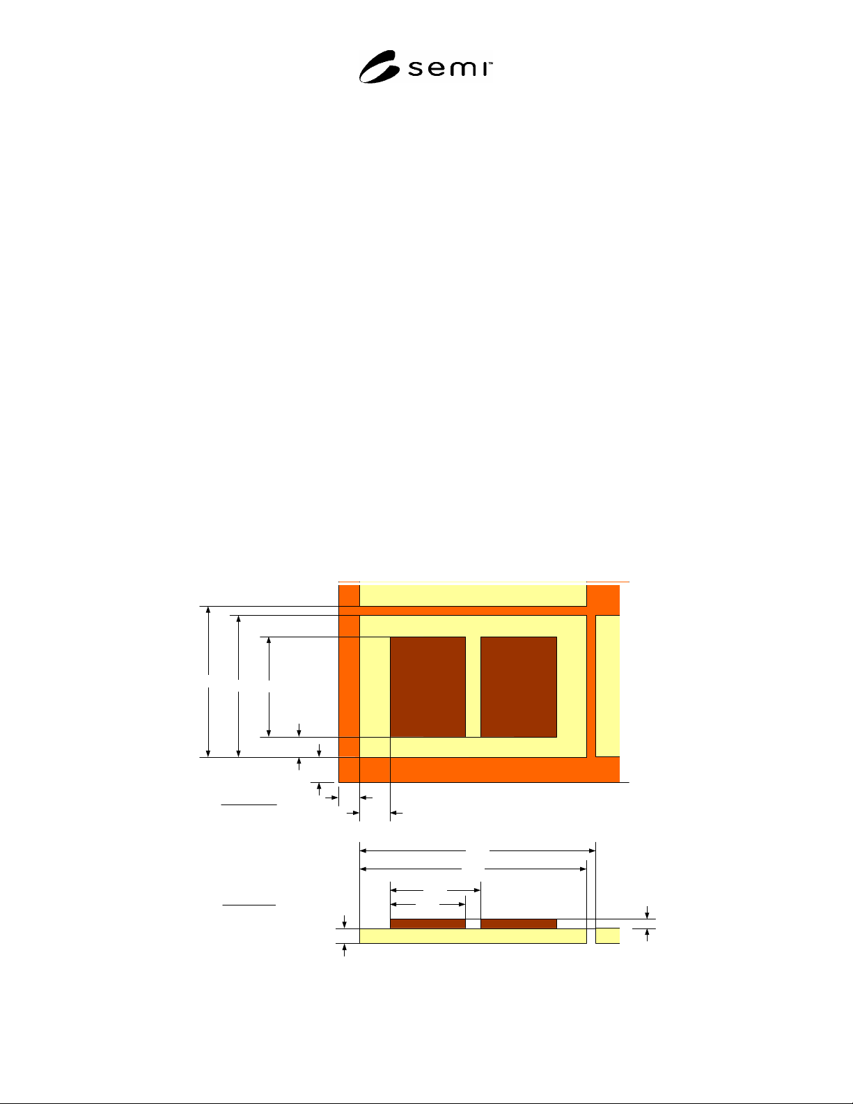
R1-3 Substrate Layout Data Report
R1-3.1 Substrate Layout Example — The following figure shows the lower left corner of a strip that contains an
array of SRAM devices with 2 Flash devices mounted on each.
R1-3.2 Layout Representation Example — The following list shows the substrate layout data that represents the
strip shown in the figure.
SRAM
FlashFlash
30.00
75.00
78.00
33.00
46.67
49.67
5.00
3.00
SRAM Layout
Dimension (X=32, Y=8)
LowerLeft (X=7.00, Y=8.33)
StepSize (X=78.00, Y=49.67)
DeviceSize (X=75.00, Y=46.67)
Height = 5.00
ZOrder = 0
25.00
7.00
8.33
Flash Layout
Dimension (X=2, Y=1)
LowerLeft (X=10.00, Y=6.67)
StepSize (X=30.00, Y=0.00)
DeviceSize (X=25.00, Y=33.0)
Height = 3.00
ZOrder = 1
6.67
10.00
Figure R1-3