semi合集-English.pdf - 第42页
SEMI E1.9-0701 E2 © SEMI 1994, 2004 22 RELATED INFORMATION 1 NOTE: This related information is not an official par t of SEMI E1.9, and it is not intended to modify or supersede the standard in any way. This information w…
SEMI E1.9-0701
E2
© SEMI 1994, 2004 21
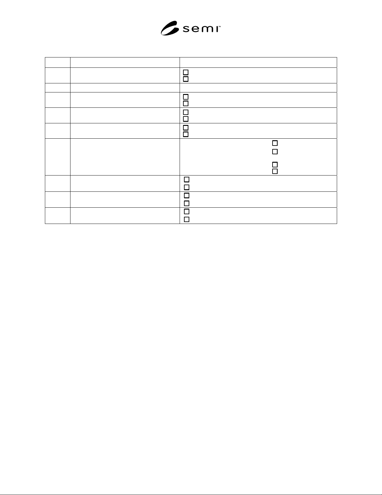
Table A1-1 Open Cassette Optional Features Checklist
Section Optional Feature Choice
6.9 carrier capacity (c)
13 wafers or
25 wafers
6.7.4 slant on 2 required fork-lift pick-up areas
angle ω = ____ (0° ≤ ω ≤ 2°)
6.4 4 robotic handling flanges
yes or
no
6.3 4 pentagonal side grip pits
yes or
no
6.7.1 features that prevent wafer creep-out
yes or
no
6.1 full 15 mm lead in provided by 3 features
that mate with kinematic coupling pins
primary kinematic coupling pins
yes or
no
and
secondary kinematic coupling pins
yes or
no
6.8.1 top cassette identification tag area
yes or
no
6.8.3 bottom cassette identification tag area
yes or
no
6.8.2 side cassette identification tag area (on front
right side domain)
yes or
no
NOTICE: These standards do not purport to address safety issues, if any, associated with their use. It is the
responsibility of the user of these standards to establish appropriate safety and health practices and determine the
applicability of regulatory limitations prior to use. SEMI makes no warranties or representations as to the suitability
of the standards set forth herein for any particular application. The determination of the suitability of the standard is
solely the responsibility of the user. Users are cautioned to refer to manufacturer' s instructions, product labels,
product data sheets, and other relevant literature respecting any materials mentioned herein. These standards are
subject to change without notice.
The user' s attention is called to the possibility that compliance with this standard may require use of copyrighted
material or of an invention covered by patent rights. By publication of this standard, SEMI takes no position
respecting the validity of any patent rights or copyrights asserted in connection with any item mentioned in this
standard. Users of this standard are expressly advised that determination of any such patent rights or copyrights, and
the risk of infringement of such rights are entirely their own responsibility.

SEMI E1.9-0701
E2
© SEMI 1994, 2004 22
RELATED INFORMATION 1
NOTE: This related information is not an official part of
SEMI E1.9, and it is not intended to modify or supersede the
standard in any way. This information was inserted by the
North America Physical Interfaces and Carriers Committee to
alert the readers to potential changes to this provisional
standard.
R1-1 A revision ballot will be submitted to insert a
statement that application of info pads C and D are
reserved to be defined by the user (for example,
distinguishing between FEOL and BEOL carriers).
NOTICE: These standards do not purport to address
safety issues, if any, associated with their use. It is the
responsibility of the user of these standards to establish
appropriate safety and health practices and determine
the applicability of regulatory limitations prior to use.
SEMI makes no warranties or representations as to the
suitability of the standards set forth herein for any
particular application. The determination of the
suitability of the standard is solely the responsibility of
the user. Users are cautioned to refer to manufacturer' s
instructions, product labels, product data sheets, and
other relevant literature respecting any materials
mentioned herein. These standards are subject to
change without notice.
The user' s attention is called to the possibility that
compliance with this standard may require use of
copyrighted material or of an invention covered by
patent rights. By publication of this standard, SEMI
takes no position respecting the validity of any patent
rights or copyrights asserted in connection with any
item mentioned in this standard. Users of this standard
are expressly advised that determination of any such
patent rights or copyrights, and the risk of infringement
of such rights are entirely their own responsibility.
Copyright by SEMI® (Semiconductor Equipment and Materials
International), 3081 Zanker Road, San Jose, CA 95134. Reproduction o
f
the contents in whole or in part is forbidden without express written
consent of SEMI.
SEMI E2-93 © SEMI 1986, 2003 1
SEMI E2-93 (Withdrawn 1103)
SPECIFICATIONS FOR QUARTZ AND HIGH TEMPERATURE WAFER
CARRIERS
These specifications were technically reapproved by the Physical Interfaces & Carriers Committee and are
the direct responsibility of the North American Physical Interfaces & Carriers Committee. Current edition
approved by the North American Regional Standards Committee in October 1998. Initially available at
www.semi.org February 1999; to be published February 1999. Originally published in 1986; previous
published revision in 1996.
NOTICE: This document was balloted and approved
for withdrawal in 2003.
1 Scope
1.1 These specifications cover the dimensional
requirements for quartz and high temperature wafer
carriers used in processing wafers. These general
requirements assist in the compatibility of wafer
carriers and most automated wafer processing
equipment. Wafer pre-orientation is recommended
before transferring wafers into quartz carriers to avoid
interference between the flat fiducial(s) and carrier
slots. These standards are intended to promote the
interchangeability of wafer carriers and encourage the
production of equipment suitable to a greater
percentage of the market.
1.2 The design definitions of SEMI Wafer Carrier
Specifications assume compliance to wafer dimensions
defined in SEMI M1, M3, or M9. For a wafer carrier to
be said to “meet the SEMI specifications,” it must be
manufactured within the dimensional limits of the given
specification, and in addition be dimensionally stable
within specification when used in accordance with
manufacturer' s recommendations. Since wafer carriers
are manufactured from a number of different raw
materials and several different manufacturing methods,
it is up to each manufacturer to determine the
recommended usage for each wafer carrier type. The
specifications were not established nor do they
represent or suggest a means to obtain any ideal
efficiencies in wafer processing results or quality of end
product.
1.3 For referee purposes, SI (System International,
commonly called metric) units shall be used for 80 mm
and larger diameter wafers.
2 Selected Definitions
2.1 For illustrations of terms, see Figure 1 for Carrier
Style 1, and Figure 2 for Carrier Style 2. Dimensions
and tolerances are given in Table 1 of the standards for
carriers of the appropriate wafer diameter.
2.1.1 base — the material at the bottom of the carrier
that the carrier rests on when placed on a flat reference
surface.
2.1.2 bottom plane — a horizontal plane tangent to the
base.
2.1.3 end — either end of carrier parallel to wafer
plane.
2.1.4 lift access — the clearance space used to insert an
implement to pick up a wafer carrier.
2.1.5 side — either one of the sides perpendicular to
the wafer plane.
3 Dimension Definitions
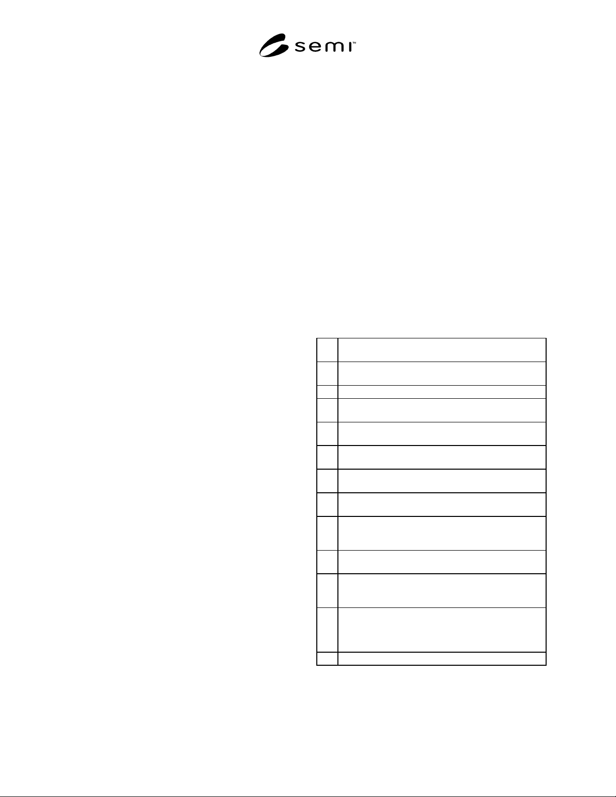
Symbol
A
Wafer Height — distance from the horizontal center line
of the wafer to the bottom plane
B
Base Width — the outside dimension of the base from
side to side
C Base Length — length of the base from end to end
D
Lift Access Height — distance from horizontal
centerline of lift access opening to bottom plane
E
Lift Access Spacing — distance from center line to
center line of lift access opening
F
Lift Access Opening — size of opening for the insertion
of an implement to pick up the carrier
G
Base End to First Slot — the distance from either end of
the carrier to the first slot on same end
H
Slot Spacing — the distance from the center line of one
slot to the center line of the adjacent slot
I
End Slot to other End Slot — the center line of the first
slot on either end to the center line of the slot on the
other end
J
Pocket Size — the diameter of a circle coincident to the
bottom of all wafer slots in a wafer position
K
Base Side to Wafer Center line — horizontal distance
from the vertical wafer center line to either side of the
base
L
Carrier Region — region enclosed by the greatest
included angle between a line drawn from the center
point of the wafer and the outermost member of the
carrier on one side and a similar line on the other side
P Separation — separation of wafers when placed in slots