semi合集-English.pdf - 第5820页
SEMI P25-94 © SEMI 1994, 2004 6 NOTICE: SEMI makes no warranties or represen tations as to the suitability o f the standards set forth herein for any particular application. The determination of the suitability of the st…
SEMI P25-94 © SEMI 1994, 2004 5
b. Alternatively, if point-like objects are available in
the image for evaluation, the focal surface may be
obtained by finding the z displacement for the best
processed point image at each image site.
6.10.1 This focal surface is reported as a map of z
displacements as a function of image position. This
map is the curvature of field.
6.10.2 The difference between the minimum z
displacement in the focal surface and the maximum z
displacement in the focal surface is the maximum
curvature of field.
NOTE 21: This includes optical image curvature, wafer
curvature, fixture curvature, etc. This procedure for the sake
of simplicity does not separate these effects. It is an error to
consider this measure of field flatness equivalent to a measure
of the optical image focal surface.
7 Report
7.1 The depth of focus, best focus, etc. reports will
include a description of the practical use, per definition
5.1.5. In addition, the report should include mention of
any special mechanical considerations — in particular,
among others, mention should be made if a chip
leveling scheme is used and whether this scheme is site
by site or global.
7.2 List of report contents:
Process: substrate and layer types and processing,
exposure conditions
Pattern: description or diagram of the test
structures, including the choice of S and T or X and
Y orientations
Wafer: the wafer quality and specifications.
Leveling: leveling mechanism.
Sites: list or map of the image sites.
Criteria: the acceptance criteria used in the
evaluation of the test structures.
Depth of Focus or Focal Range (single overall
values)
Best Focus (single overall value)
Astigmatism map
Maximum Astigmatism
Mean Astigmatism
Field Flatness map
Maximum Curvature of Field
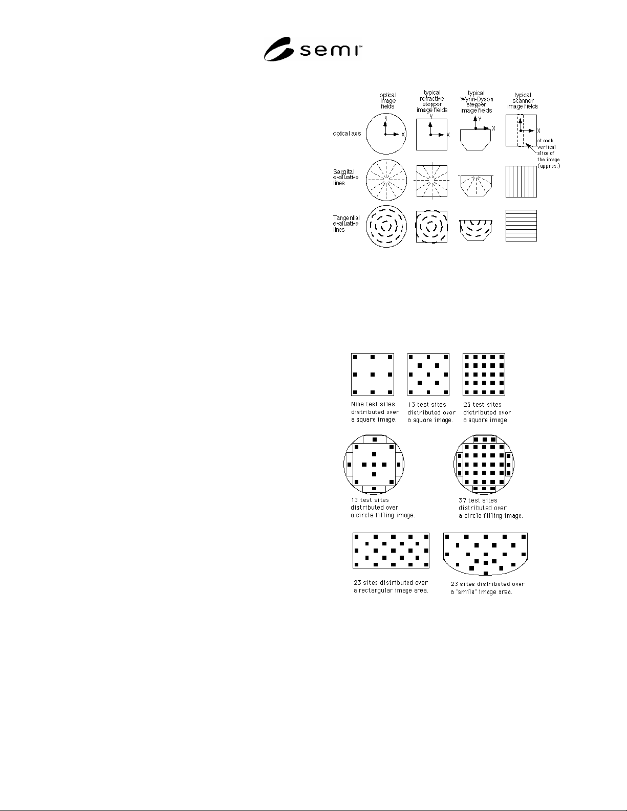
Figure 1
The Coordinate System and the Sagittal and
Tangential Lines, Shown for the Optical Image
Cylindrical Symmetry and for the Actual
Processed Images of Steppers and Scanners
Figure 2
Typical Test Site Placements in
Various Types of Image Fields

SEMI P25-94 © SEMI 1994, 2004 6
NOTICE: SEMI makes no warranties or representations as to the suitability of the standards set forth herein for any
particular application. The determination of the suitability of the standard is solely the responsibility of the user.
Users are cautioned to refer to manufacturer's instructions, product labels, product data sheets, and other relevant
literature, respecting any materials or equipment mentioned herein. These standards are subject to change without
notice.
By publication of this standard, Semiconductor Equipment and Materials International (SEMI) takes no position
respecting the validity of any patent rights or copyrights asserted in connection with any items mentioned in this
standard. Users of this standard are expressly advised that determination of any such patent rights or copyrights, and
the risk of infringement of such rights are entirely their own responsibility.
Copyright by SEMI® (Semiconductor Equipment and Materials
International), 3081 Zanker Road, San Jose, CA 95134. Reproduction of
the contents in whole or in part is forbidden without express written
consent of SEMI.

SEMI P26-0703 © SEMI 1996, 2003 1
SEMI P26-0703
PARAMETER CHECKLIST FOR PHOTORESIST SENSITIVITY
MEASUREMENT
This checklist was technically approved by the Global Micropatterning Committee and is the direct
responsibility of the Japanese Micropatterning Committee. Current edition approved by the Japanese
Regional Standards Committee on April 28, 2003. Initially available at www.semi.org June 2003; to be
published July 2003. Originally published in 1996.
1 Purpose
1.1 This checklist identifies the parameters for the
measurement of photoresist sensitivity in order to avoid
the variations between the supplier and users of
photoresist.
2 Scope
2.1 The resists for which this guideline is intended are
positive photoresist.
2.2 In discussions between the supplier and the user of
the resists, quantitative values should be provided for
each parameter.
NOTICE: This standard does not purport to address
safety issues, if any, associated with its use. It is the
responsibility of the users of this standard to establish
appropriate safety and health practices and determine
the applicability of regulatory or other limitations prior
to use.
3 Referenced Standards
3.1 SEMI Standard
SEMI P27 — Parameter Checklist for Resist Thickness
Measurement on a Substrate
3.2 ASTM
1
ASTM F1059 — Practice for Calculating the Contrast
and Threshold Sensitivity of a Positive Photoresist
NOTICE: Unless otherwise indicated, all documents
cited shall be the latest published versions.
4 Terminology
4.1 Definitions
4.1.1 E
op
(optimum energy) — the exposure energy
where the mask dimensions can be reproduced
faithfully.
1 American Society for Testing and Materials, 100 Barr Harbor
Drive, West Conshohocken, Pennsylvania 19428-2959, USA.
Telephone: 610.832.9585, Fax: 610.832.9555, Website:
www.astm.org
4.1.2 E
th
(threshold energy) — the exposure energy
where the remained thickness ratio becomes zero on the
sensitivity curve.
5 Parameters
5.1 Substrate — Silicon wafer
5.2 Pre-Treatment of Substrate
5.2.1 Removal of native oxide on silicon wafer is
recommended.
5.2.2 Describe the process when the surface of silicon
wafer has been treated with HMDS.
5.3 Resist
5.3.1 Trade-name of photoresist.
5.3.2 Film thickness after prebake. (Recommended
thickness is 1.0–1.2 µ m.)
5.4 Prebake Condition
5.4.1 Type of equipment for prebake; contact or
proximity-bake.
5.4.2 Measuring position of the temperature in baking
equipment and equipment for temperature measuring.
5.4.3 Baking time (s).
5.4.4 Program sequence.
5.5 Exposure
5.5.1 Type of exposure machine; stepper or mirror
projection.
5.5.2 Wavelength and half width (nm).
5.5.3 Light intensity of the exposed surface (mW/cm
2
).
5.5.4 Numerical Aperture and sigma value.
5.6 Post-Exposure Bake (if performed)
5.6.1 Type of equipment for post-exposure bake;
contact or proximity-bake.
5.6.2 Measuring position of the temperature in baking
equipment and equipment for temperature measuring.
5.6.3 Baking time (s).
5.6.4 Program sequence.