semi合集-English.pdf - 第7446页
SEMI MF1535-1104 © SEMI 2004 4 minority and majority carrier capture time co nstants (see Related Info rmation 1). 5.1.3 surface recombination velocity — a m easure of the recombination of excess minority carriers at the…

SEMI MF1535-1104 © SEMI 2004 3
(such as a wafer with oxide precipitates and a surface
denuded region free of such precipitates).
3.5 The recombination characteristics of impurities in
silicon are strongly temperature dependent. If
comparisons between measurements are to be made
(that is, before and after a process step or at a supplier
and a customer), both measurements should be made at
the same temperature.
3.6 Different impurity centers have different
recombination characteristics. Therefore, if more than
one type of recombination center is present in the
wafer, the decay may consist of contributions with two
or more time constants. The recombination lifetime
deduced from such a decay curve may not be
representative of any of the individual centers.
3.7 The recombination characteristics of an impurity
center depend on the dopant type and density of the
wafer as well as the position of the energy level of the
impurity center in the forbidden energy gap (see
Related Information 3).
4 Referenced Standards
4.1 SEMI Standards
SEMI C28 — Specifications and Guidelines for
Hydrofluoric Acid
SEMI C35 — Specifications and Guideline for Nitric
Acid
SEMI M1 — Specifications for Polished
Monocrystalline Silicon Wafers
SEMI M20 — Practice for Establishing a Wafer
Coordinate System
SEMI MF28 — Test Methods for Minority-Carrier
Lifetime in Bulk Germanium and Silicon by
Measurement of Photoconductive Decay
SEMI MF42 — Test Methods for Conductivity Type of
Extrinsic Semiconducting Materials
SEMI MF84 — Test Method for Measuring Resistivity
of Silicon Wafers With an In-Line Four-Point Probe
SEMI MF391 — Test Methods for Minority Carrier
Diffusion Length in Extrinsic Semiconductors by
Measurement of Steady-State Surface Photovoltage
SEMI MF533 — Test Method for Thickness and
Thickness Variation of Silicon Slices
SEMI MF673 — Test Methods for Measuring
Resistivity of Semiconductor Slices or Sheet Resistance
of Semiconductor Films with a Non-contact Eddy-
Current Gage
SEMI MF723 — Practice for Conversion Between
Resistivity and Dopant Density for Boron-Doped,
Phosphorus-Doped, and Arsenic-Doped Silicon
SEMI MF978 — Test Method for Characterizing
Semiconductor Deep Levels by Transient Capacitance
Techniques
SEMI MF1241 — Terminology of Silicon Technology
SEMI MF1388 — Test Methods for Generation
Lifetime and Generation Velocity of Silicon Material
by Capacitance-Time Measurements of Metal-Oxide-
Silicon (MOS) Capacitors
SEMI MF1530 — Test Method for Flatness, Thickness,
and Thickness Variation of Silicon Wafers by
Automated Noncontact Scanning
4.2 ASTM Standard
D 5127 — Guide for Ultra Pure Water Used in the
Electronics and Semiconductor Industry
7
4.3 DIN Standard
DIN 50 440 Part 1 — Measurement of Carrier Lifetime
in Silicon Single Crystals: Carrier Recombination
Lifetime at Low Injection by Photoconductivity Decay
8
NOTICE: Unless otherwise indicated, all documents
cited shall be the latest published versions.
5 Terminology
5.1 Definitions
5.1.1 injection level — the ratio of the density of
excess carriers generated by photons or other means to
the equilibrium density of majority carriers in an
extrinsic semiconductor crystal or wafer.
5.1.2 recombination lifetime — the average time
interval between the generation and recombination of
hole-electron pairs in a homogeneous semiconductor.
5.1.2.1 Discussion — In the Shockley-Read-Hall
model, which applies for a small density of
recombination centers, the recombination lifetime for
centers with energy levels that are not too close to a
band edge is the minority-carrier capture time constant
provided that the density of excess carriers is very small
compared with the density of majority carriers (low
injection). When the density of injected carriers greatly
exceeds the density of the majority carriers (high
injection), the recombination lifetime is the sum of the
7 Annual Book of ASTM Standards, Vol 11.01, ASTM International,
100 Barr Harbor Drive, West Conshohocken, PA 19428. Telephone:
610-832-9500, Fax: 610-832-9555, Website:
www.astm.org.
8 Available in both German and English editions from Deutches
Institut für Normung e.V., Beuth Verlag GmbH, Burggrafenstrasse 4-
10, D 10787 Berlin, Germany, website:
www.din.de
.
SEMI MF1535-1104 © SEMI 2004 4
minority and majority carrier capture time constants
(see Related Information 1).
5.1.3 surface recombination velocity — a measure of
the recombination of excess minority carriers at the
surface of a semiconductor crystal or wafer given by
the ratio of the surface-directed hole or electron current
to the product of the hole or electron charge and hole or
electron density at the surface.
5.2 Definitions of other terms used in silicon
technology may be found in SEMI M1 and SEMI
MF1241.
6 Summary of Test Method
6.1 Excess hole-electron pairs are locally created in the
wafer for a very brief time by a short pulse (width 200
ns, rise and fall times 25 ns) of light with energy
slightly greater than the width of the forbidden energy
gap at a specified power density (injection level). The
specimen surface is conditioned in such a way that
surface recombination has a negligible effect on the
decay of the conductivity following cessation of the
light pulse. This decay is monitored by means of
microwave reflectance, and the carrier recombination
lifetime is determined as the time constant of the
appropriate portion of the exponential conductivity
decay.
6.2 A narrow-beam light source may be used so that
measurements may be made repeatedly at different
localized points on the wafer to obtain a map of the
distribution of carrier recombination lifetime.
6.3 The measurement may be repeated at several
different values of specific parameters, such as injection
level (light source intensity) or temperature in order to
obtain more detailed information about the nature of the
recombination centers.
6.4 A process step that acts as a contamination source
can sometimes be identified by comparing
measurements of carrier recombination lifetime made
before and after the step.
7 Apparatus
7.1 Pulsed Light Source — A laser diode with
wavelength between 0.9 and 1.1 m. Pulse length is
nominally 200 ns, and the rise and fall times are 25
ns (Note 2). It is preferred that the output power of the
light source be variable such that photon densities
between 2.5 10
10
and 2.5 10
15
photon/cm
2
are
generated at the wafer surface during the pulse.
NOTE 2: The rise and fall times of the pulsed light source
and the sampling time of the signal conditioner (see Section
7.5) should be 0.1 of the shortest lifetime to be measured.
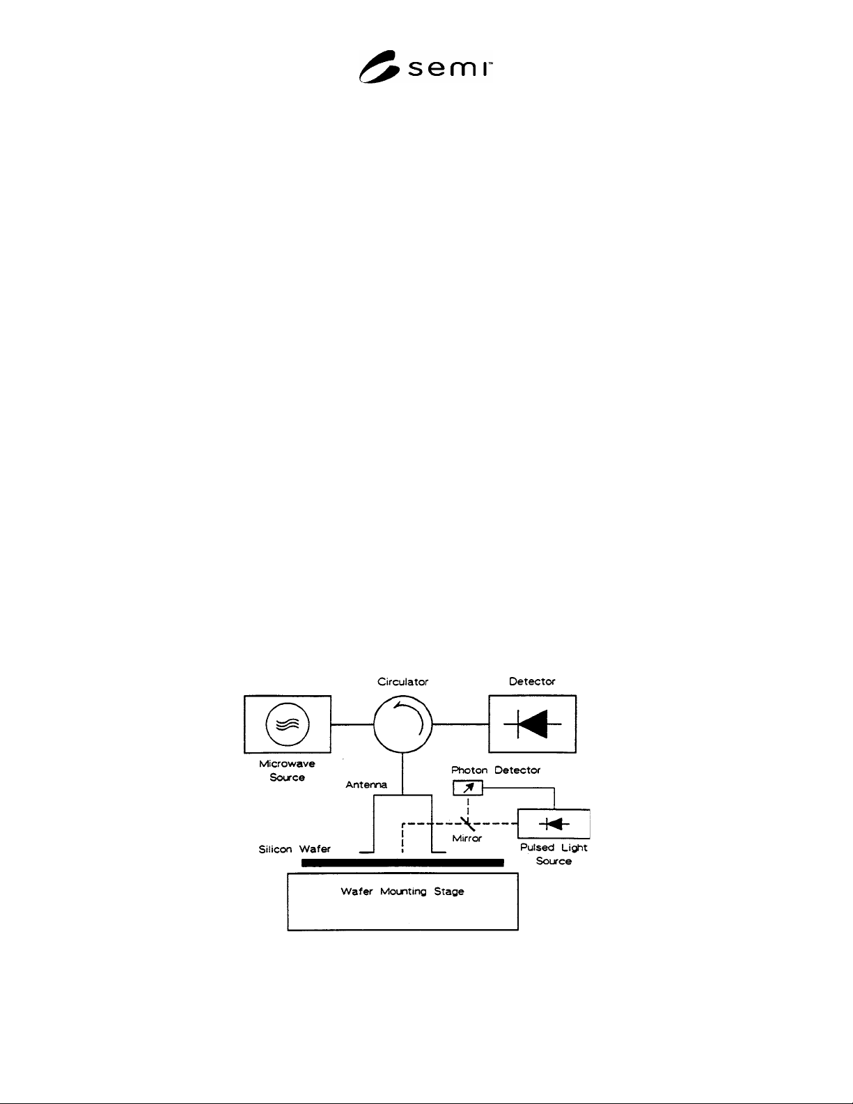
7.2 Photon Detector — Suitable means, such as a
semitransparent mirror in the light path at an angle of
45° and a silicon photodetector, to provide feedback
control to maintain the laser power at a constant level
appropriate to the specified injection level.
7.3 Microwave Pick-Up System — Including a
microwave source operating at a nominal frequency of
10 ± 0.5 GHz and an apparatus for measuring reflected
power, such as a circulator, an antenna, and a detector
(see Figure 1). The sensitivity of the detection system
shall be as great as possible to permit measurement of
photoconductivity decay at low injection levels.
Figure 1
Example Block Diagram of Pulsed Light and Microwave Systems

SEMI MF1535-1104 © SEMI 2004 5
7.4 Wafer Mounting Stage — For holding the wafer
(with vacuum hold down) in the desired position under
the pulsed light source. The stage may contain a heater
for controlling its temperature over a small temperature
range above room temperature. It may be driven by
computer controlled motors to provide x-y or r-
motion for mapping capability over the wafer surface
and may have automatic wafer loader and transport to
facilitate automatic sequential measurement of a group
of wafers.
7.5 System for Analysis of the Decay Signal —
Appropriate signal conditioners and display unit (real or
virtual oscilloscope with suitable time sweep and signal
sensitivity). The signal conditioner shall have a
bandwidth 40 MHz, or a minimum sampling time 25
ns (Note 2). The display unit shall have a continuously
calibrated time base with accuracy and linearity better
than 3%. The system shall be such that the time
constant of user-specified portions of the decay signal
can be established independently.
7.6 Computer System — Although the measurement
can be made manually, it is recommended that it be
carried out using a suitable computer system that
controls the wafer loading, stage motion, the pulse and
detector operation, decay signal analysis, statistical
analysis of the data, data logging and storage, and
printing or plotting of results.
7.7 Facilities for Etching or Passivating Wafer
Surfaces — If required.
7.7.1 For Chemical Passivation — A fume hood
equipped with an acid-proof sink and suitable beakers
or other containers for holding wet chemicals, including
hydrofluoric acid at room temperature and protective
gear appropriate to the chemicals used.
7.7.2 For Oxidation — A clean furnace capable of
high quality dry oxidations at temperatures of 950° to
1050°C and associated cleaning, drying, and wafer
handling facilities.
7.8 Wafer Holder — If required. In some cases, it may
be necessary to measure the wafer while it is immersed
in a passivating solution (see Section 11). In this case,
a flat chemically inert, optically transparent holder is
required to contain both the wafer and the passivating
solution.
8 Reagents
8.1 Purity of Reagents — All chemicals for which such
specifications exist shall conform to Grade 1 SEMI
specifications for those specific chemicals. Other
chemicals shall conform to reagent grade, as specified
in Reagent Chemicals.
9
Other grades may be used,
provided it is first determined that the chemical is of
sufficiently high purity to permit its use without
lessening the accuracy of the test.
8.2 Purity of Water — Reference to water shall be
understood to mean Type E-3 or better water as
described in ASTM Guide D 5127.
8.3 The recommended chemicals shall have the
following nominal assays:
8.3.1 Ethanol (CH
3
CH
2
OH) — Absolute, 99.9%.
8.3.2 Iodine (I
2
) — >99.8%.
8.3.3 Hydrofluoric Acid (HF) — Concentrated, 49.00 ±
0.25%. Warning: see Section 9.3 for warning
statement.
8.3.4 Nitric Acid (HNO
3
) — Concentrated, 70.0–
71.0%.
8.4 Iodine-Ethanol Passivating Solution — Mix 1 g
iodine with 100 mL ethanol.
NOTE 3: Other passivating solutions may be utilized
provided that they (1) reduce the surface recombination
velocity to a value at which surface recombination no longer
interferes with the determination of the bulk recombination
lifetime (see Section 11), and (2) result in stable surfaces (see
Section 6.2.1).
8.5 Bright Etching Solution, for Etching Non-Polished
Surfaces — Mix 95 mL concentrated HNO
3
with 5 mL
concentrated HF. Warning: See Section 9.3 for
warning statement.
8.6 Dilute HF Solution, for Etching Surface Oxide
Films — To obtain 100 mL of a 2 % solution of HF,
mix 4 mL concentrated HF with 96 mL of water.
Warning: See Section 9.3 for warning statement.
9 Hazards
9.1 The laser illumination system should be interlocked
so that direct observation of the laser beam is
prevented. Warning: Do not operate the laser
illumination system with the interlock disabled.
9.2 The microwave system should be shielded and
interlocked so that personnel cannot come into contact
with the beam. Warning: Do not operate the
microwave system with the interlock disabled.
9 Reagent Chemicals, American Chemical Society Specifications,
American Chemical Society, Washington, DC. For suggestions on
the testing of reagents not listed by the American Chemical Society,
see Analar Standards for Laboratory Chemicals, BDH Ltd., Poole,
Dorset, U.K., and the United States Pharmacopeia and National
Formulary, U.S. Pharmacopeial Convention, Inc. (USPC),
Rockville, MD.