semi合集-English.pdf - 第6550页
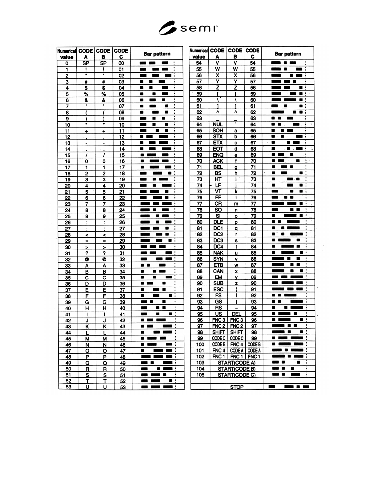
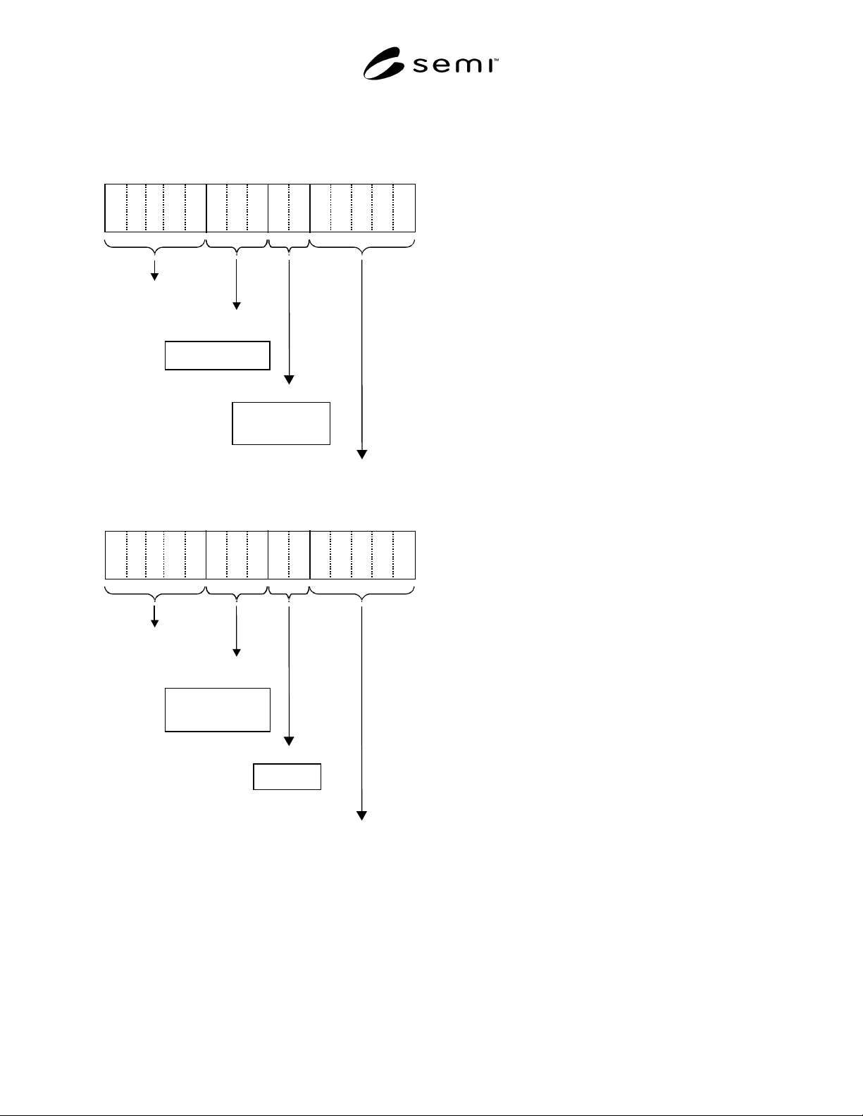
SEMI G83-0301 © SE MI 2001 6 A1-3 Example of Data Contents A1-3.1 The i tems sh o wn in Figu res A1-3 and A1- 4 are data contents of bar code that comply with this specification. Manufacturi ng Date Sub-Lot No. Product R…
SEMI G83-0301 © SEMI 20015
Figure A1-2
AIM USS-128
SEMI G83-0301 © SEMI 2001 6
A1-3 Example of Data Contents
A1-3.1 The items shown in Figures A1-3 and A1-4 are
data contents of bar code that comply with this
specification.
Manufacturing
Date
Sub-Lot No.
Product
Recognition
No.
Hexadecimal:
#109
Lot No.
November 20, 1999
ZDR11N9BK6 TX024
Figure A1-3
Example of Data Contents
Manufacturing
Date
Sub-Lot No.
Product
Recognition
N
o.
unused
Lot No.
N
ovember, 1999
Z-R11N9B-- TX024
( Date unused )
Figure A1-4
Example of Data Contents
NOTICE: SEMI makes no warranties or representa-
tions as to the suitability of the standard set forth herein
for any particular application. The determination of the
suitability of the standard is solely the responsibility of
the user. Users are cautioned to refer to manufacturer’s
instructions, product labels, product data sheets, and
other relevant literature respecting any materials or
equipment mentioned herein. These standards are
subject to change without notice.
The user’s attention is called to the possibility that
compliance with this standard may require use of
copyrighted material or of an invention covered by
patent rights. By publication of this standard, SEMI
takes no position respecting the validity of any patent
rights or copyrights asserted in connection with any
item mentioned in this standard. Users of this standard
are expressly advised that determination of any such
patent rights or copyrights, and the risk of infringement
of such rights, are entirely their own responsibility.
Copyright by SEMI® (Semiconductor Equipment and Materials
International), 3081 Zanker Road, San Jose, CA 95134. Reproduction o
f
the contents in whole or in part is forbidden without express written
consent of SEMI.

SEMI G84-0303 © SEMI 2001, 2003 1
SEMI G84-0303
SPECIFICATION FOR STRIP MAP PROTOCOL
This specification was technically approved by the Global Automated Test Equipment Committee and is the
direct responsibility of the North American Automated Test Equipment Committee. Current edition approved
by the North American Regional Standards Committee on October 25, 2002 and November 22, 2002.
Initially available at www.semi.org January 2003; to be published March 2003. Originally published
November 2001.
1 Purpose
1.1 The purpose of this specification is to provide
definition that will enable the implementation of strip
mapping throughout the assembly and test process. This
document will enable standardization of the strip map
format and execution method throughout the factory
floor.
1.2 This document describes the format and methods in
which strip map information shall be formatted and
used to transfer information about a strip to and from
equipment using the SECS/GEM interface standard (see
SEMI E5).
2 Scope
2.1 This specification will identify the messages within
the SECS/GEM message set used in the implementation
of strip mapping.
2.2 This specification will identify the Map Data Items
(MDI) that are required or optionally may be used in
the implementation of strip mapping.
2.3 This document will provide basic application notes
to aid in the proper implementation of strip mapping.
2.4 This document will not address application or
implementation for wafer test process.
NOTICE: This standard does not purport to address
safety issues, if any, associated with its use. It is the
responsibility of the users of this standard to establish
appropriate safety and health practices and determine
the applicability of regulatory or other limitations prior
to use.
3 Limitations
3.1 This document does not address the transmission,
file naming conventions, storage or archiving of strip
maps.
4 Referenced Standards
4.1 SEMI Standards
SEMI E5 — SEMI Equipment Communications
Standard 2 Message Content (SECS-II)
SEMI G81
— Specification for Map Data Items
SEMI T9 — Specification for Marking of Metal Lead-
Frame Strips with a Two-Dimensional Data Matrix
Symbol
NOTICE: Unless otherwise indicated, all documents
cited shall be the latest published versions.
5 Terminology
5.1 Definitions
5.1.1 assembly site — the sub-contractor, supplier’s
facility or department that will be responsible for the
assembly of IC devices.
5.1.2 bottom-side — the bottom of the strip as defined
by the customer based on the customer master
manufacturing drawing.
5.1.3 cell — a term used to represent the mapping item
on a strip—unit, package, device, multi-chip module,
etc.
5.1.4 strip — a leadframe, board, panel or other
container which hold locations for semiconductor
devices to be manufactured upon.
5.1.5 strip map — a record of data in a file that
contains quality and historical information about each
individual strip in a manufacturers lot.
5.1.6 substrate — a board or panel containing locations
for semiconductor devices to be manufactured upon.
Also referred to as strip, board or PCB.
5.1.7 supplier — a supplier of inspected/tested
substrates (strips) and strip maps to the assembly site.
5.1.8 top-side — the top of the strip as defined by the
customer based on the customer master manufacturing
drawing.
6 Ordering Information
None.
7 Convention
7.1 The following conventions are used to represent
data format. Each format is represented by an
alphabetic character and optional data size given by
“byte” unit. Exceptions are “*” and “List of”. Refer to
SEMI E5 for details.