semi合集-English.pdf - 第730页
SEMI E99-1104 E © SEMI 2000, 2004 20 RELATED INFORMATION 4 NOTICE : This relat ed information is not an official part of S EMI E99 and was derived from the Japanese Information and Control Committee. Th is related inform…
SEMI E99-1104
E
© SEMI 2000, 2004 19
RELATED INFORMATION 3
APPLICATION NOTES
NOTICE: This related information is not an official part of SEMI E99. This related information was approved for
publication by full letter ballot procedures on September 3, 1999.
R3-1 Combined State Model
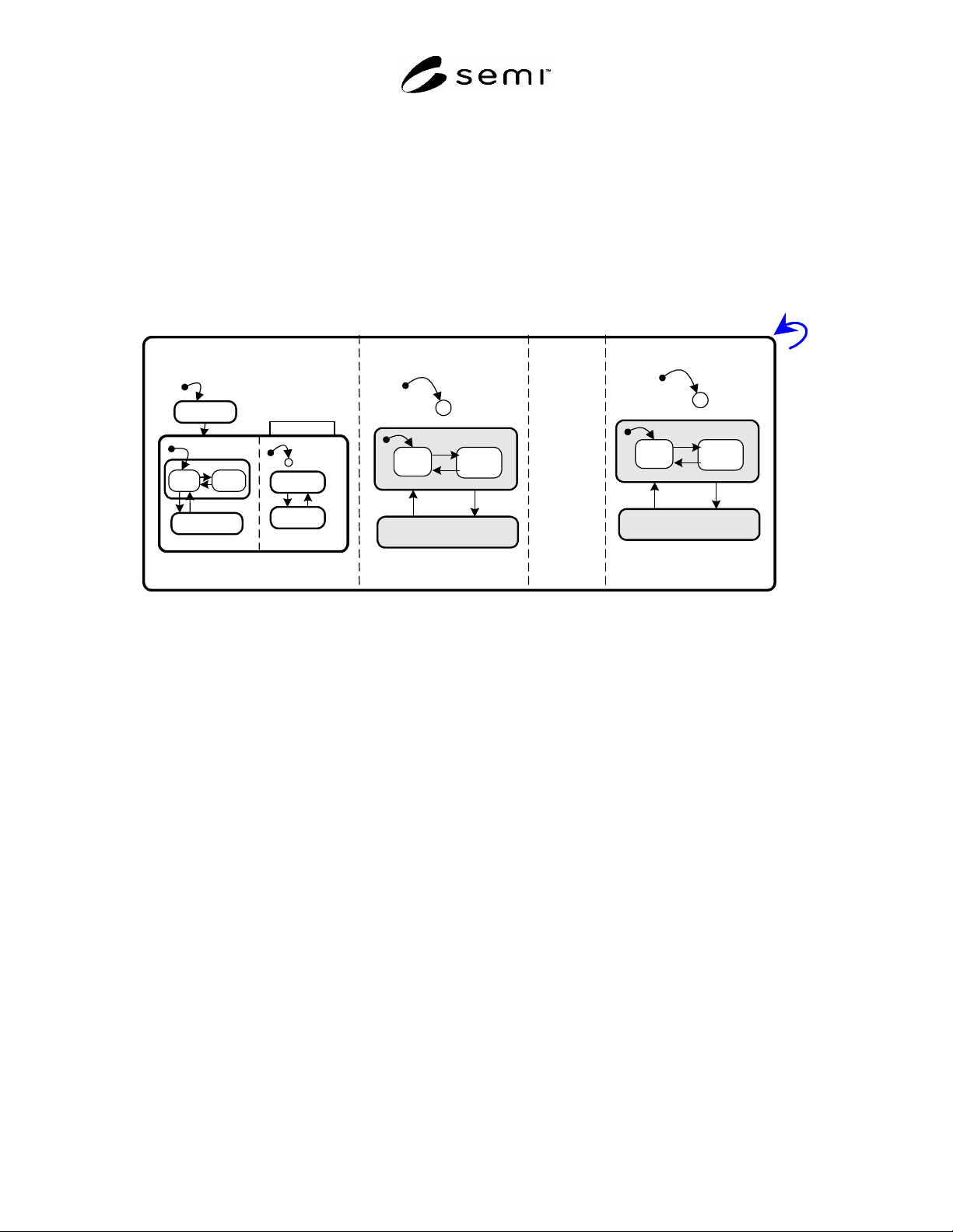
R3-1.1 The following figure, R3-1 shows the combined state model for the CIDRW unit with nn heads, from
HEAD01 TO HEADnn. The CIDRW is considered as IDLE when and only when it is in OPERATING and all of
its heads are IDLE.
CIDRW
HEAD01
C
12
OPERATING
16
BUSY
IDLE
13
14
15
NOT OPERATING
C
12
HEADnn
11
1
INITIALIZING
3
2
NO
ALARMS
ALARMS
MAINTENANCE
4
5
910
ALARM STATUSOPERATIONAL
RUNNING
IDLE
7
8
6
BUSY
OPERATING
C
OPERATING
16
BUSY
IDLE
13
14
NOT OPERATING
15
.....
Figure R3-1
Combined State Model
SEMI E99-1104
E
© SEMI 2000, 2004 20
RELATED INFORMATION 4
NOTICE: This related information is not an official part of SEMI E99 and was derived from the Japanese
Information and Control Committee. This related information was approved for publication by full letter ballot on
January 10, 2003.
R4-1 Application of RF Tag as Carrier ID Tag
R4-1.1 In case that RF Tag is utilized as Carrier Tag for SEMI E99 application, to secure the interoperability among
the CIDRW units for writing / reading the Carrier ID into / out of the RF Tag, some basic consideration should be
taken as follows:
R4-1.1.1 Coincidence of Carrier ID Written and Read in Tag Memory — Fundamentally Carrier ID, which is read
out, should be quite same as written, with no addition.
R4-1.1.2 Caution for Carrier ID Contents Applied to Object ID — Carrier ID as Material ID can be used as Object
ID. But the Space Character (20
16
) should not be used as the first or the last character of Carrier ID. SEMI E39
restricts these.
R4-1.1.3 Non-Visible Character in Carrier ID — If non-visible ASCII character is found within the specified tag
area, CIDRW shall send out an error (i.e. Execution error) to the upstream controller when “Read ID” service was
executed. The contents of Carrier ID issued by host/upstream controller should be compliant with visible Character.
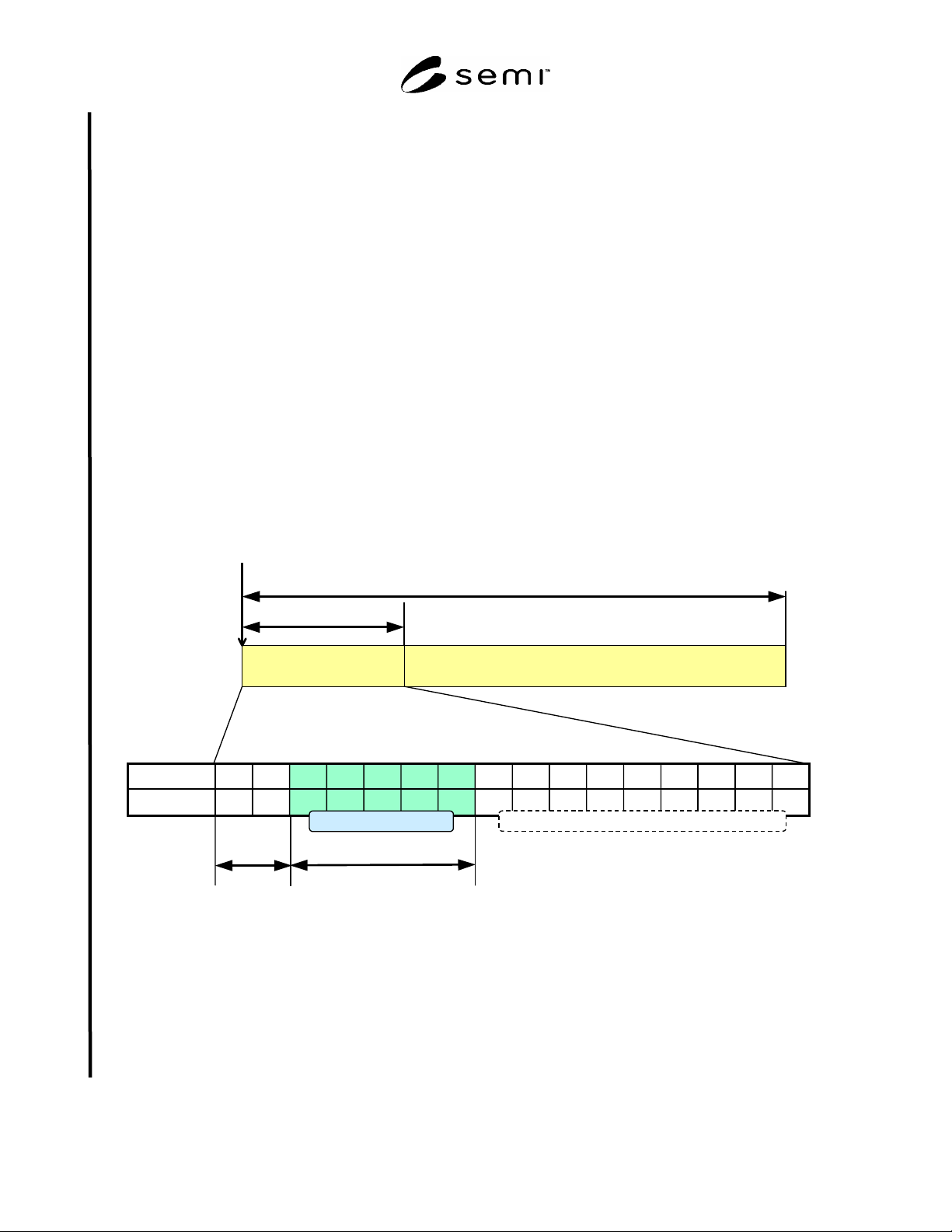
R4-1.1.4 Location of Carrier ID Field (CID Field) — Carrier ID field shall be located from the first byte to the
maximum byte of Carrier ID in the memory of the Electric Tag. The relation of Carrier ID Offset and Carrier ID
length are shown bellow:
CID Field
First Byte
Maximum Byte of CID
Total Tag Length
141312111009
E
06
D
05
C
04
B
03 07
A
02
NUL
01
NUL
00 1508
ASCII
Address 141312111009
E
06
D
05
C
04
B
03 07
A
02
NUL
01
NUL
00 1508
ASCII
Address
Offset
Length
Do Not Care
CID
Figure R4-1
Example of Carrier ID in Tag (“CID = ABCDE”)
R4-1.1.5 Condition of CarrierIDOffset and CarrierIDLength —
By setting the condition of CarrierIDOffset and
CarrierIDLength, CIDRW can correspond to CarrierID Tag characteristic to device makers already existing, if they
are compliant with the reinforced specification for RF Tag in SEMI E99.
R4-1.1.5.1 The information of the Offset value and Length of Carrier ID should be stored as the CIDRW Attribute.
R4-1.1.5.2 When a CIDRW is installed in the equipment, it needs to set up a condition of CarrirIDOffset and
CarrierIDLength as per user requirement once at least.

SEMI E99-1104
E
© SEMI 2000, 2004 21
NOTICE: SEMI makes no warranties or representations as to the suitability of the standard set forth herein for any
particular application. The determination of the suitability of the standard is solely the responsibility of the user.
Users are cautioned to refer to manufacturer’s instructions, product labels, product data sheets, and other relevant
literature respecting any materials mentioned herein. These standards are subject to change without notice.
The user’s attention is called to the possibility that compliance with this standard may require use of copyrighted
material or of an invention covered by patent rights. By publication of this standard, SEMI takes no position
respecting the validity of any patent rights or copyrights asserted in connection with any item mentioned in this
standard. Users of this standard are expressly advised that determination of any such patent rights or copyrights, and
the risk of infringement of such rights, are entirely their own responsibility.
Copyright by SEMI® (Semiconductor Equipment and Materials
International), 3081 Zanker Road, San Jose, CA 95134. Reproduction of
the contents in whole or in part is forbidden without express written
consent of SEMI.