semi合集-English.pdf - 第7267页
SEMI MF671-0705 © SEMI 2003, 2005 4 10.2 Identify near t he horizontal reference line the projected im age of a point on the sample stage. A defect or a particle of dust will serve this purpos e. This projected imag e sh…
SEMI MF671-0705 © SEMI 2003, 2005 3
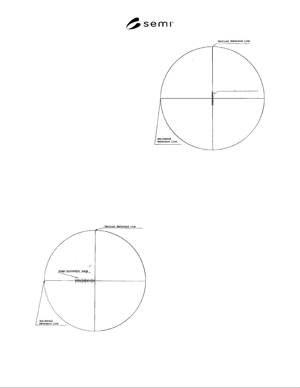
7.1.4 An overlay, with reference lines perpendicular to
each other intersecting at the center, and ten calibrated
divisions on the vertical reference line above and below
center, corresponding to 50 m (0.002 in.) per division at
the sample location. See Figure 1.
NOTE 2: For a 20× overlay, the calibration divisions on the
overlay itself are 1 mm apart.
7.2 Microscope Stage Micrometer — On clear glass or
plastic, the scale to be at least 1.3 mm (0.05 in.) long with
25 m (0.001 in.) divisions.
7.3 Machinists’ Steel Scale — 150 mm (or 6 in.)
minimum length, graduated in 0.50 mm (0.02 in.) or
0.25 mm (0.01 in.).
8 Sampling
8.1 Unless otherwise specified, ASTM Practice E 122
shall be used. When so specified, appropriate sample
sizes shall be selected from each lot in accordance with
ANSI/ASQC Z1.4–1993. Inspection levels shall be
agreed upon between the supplier and purchaser.
9 Calibration
9.1 Comparator Optical Magnification
9.1.1 Place the microscope stage micrometer on the comparator sample stage so that its projected image is at the
center of the viewing screen.
9.1.2 With a steel scale on the viewing screen, count the number of 25 m (0.001 in.) lines projected over a 25 mm
(or 1 in.) distance. Divide the number into 1000 to obtain the actual magnification.
9.1.3 Magnification must be between 19.8 and 20.2 to be usable for this method.
9.2 Comparator Micrometer Travel — x Direction
9.2.1 Set the x-travel micrometer to zero.
9.2.2 Align the projected image of the microscope stage
micrometer such that the array of scale division lines is
horizontal and the right most lines are all to one side of
the vertical reference line on the viewing screen as in
Figure 2.
9.2.3 Using the x-travel micrometer, scan the image of
the microscope stage micrometer until the array has been
transposed to the opposite side of the vertical reference
line in an analogous manner.
9.2.4 Read the x-travel micrometer scale. This value
should agree with the full-range value of the microscope
stage micrometer scale within 25 m (0.001). If the value
does not agree, adjust or repair the micrometer.
10 Procedure
10.1 Mount the overlay (see Figure 1) on the viewing
screen. Position the horizontal reference line
approximately parallel to the floor.
Figure 2
Calibration of the Horizontal Travel
Comparator Stage
Figure 1
Overlay
calibrated divisions
SEMI MF671-0705 © SEMI 2003, 2005 4
10.2 Identify near the horizontal reference line the projected image of a point on the sample stage. A defect or a
particle of dust will serve this purpose. This projected image should be no larger than one-half division on the
overlay scale.
10.3 Align the horizontal reference line to the x-axis travel by repeatedly scanning the point identified in ¶10.2 and
manipulating the overlay and the x-y movement of the sample stage. Alignment is achieved when this point is
centered on the horizontal reference line when scanned from one edge of the viewing screen to the other.
10.4 Place the wafer on the stage so that the central portion of the projected image of the flat is centered on the
viewing screen and is coincident with the horizontal reference line.
10.5 Visually fit the projected image of the flat to the horizontal reference line.
10.5.1 Scan from one end of the flat to the other using the x-axis micrometer.
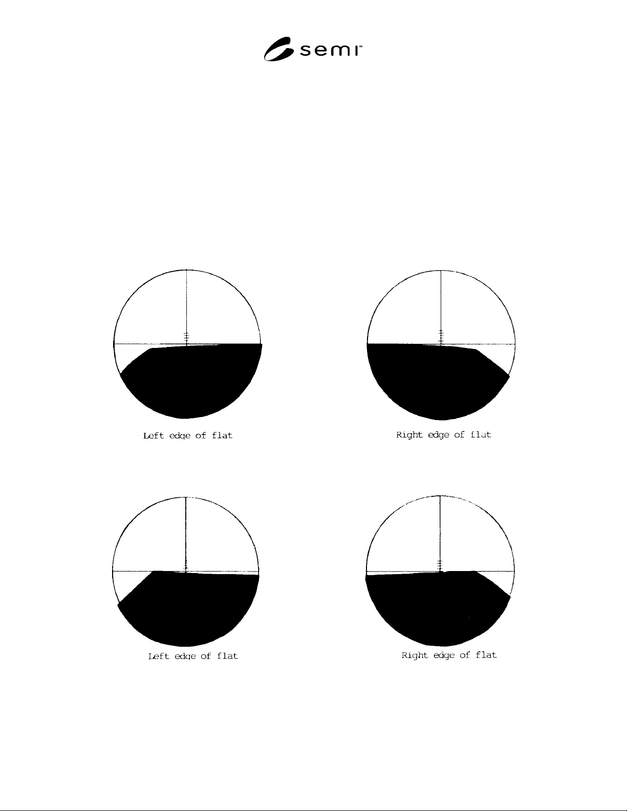
10.5.2 If the apparent shape of the flat is convex, adjust the goniometer and micrometers, while repeating ¶10.5.1
such that the high point is contacting the reference line and the low points are equidistant from the reference line.
See Figure 3.
Figure 3
Aligning a Convex Shaped Flat
10.5.3 If the apparent shape of the flat is concave, adjust the goniometer and micrometers, while repeating ¶10.5.1
such that the high points are contacting the reference line. See Figure 4.
Figure 4
Aligning a Concave Shaped Flat
10.6 Adjust the projected image of the flat using the x-axis micrometer so that the left end is coincident with the
intersection of the vertical and horizontal reference lines.

SEMI MF671-0705 © SEMI 2003, 2005 5
10.7 To determine the location of the end of the flatted
region, use the point at which the wafer image on the
comparator screen is one division away from the horizontal
reference line. This corresponds to an offset of 50 m
(0.002 in.) on the wafer. (See Figure 5.)
10.8 Record the micrometer reading to the nearest 25 m or
0.001 in. as E
l
(left) on the data sheet (see example in
Figure 6).
10.9 Scan the projected image of the flat using the x-axis
micrometer so that the right end is coincident with the
intersection of the vertical and horizontal reference lines.
10.10 Determine the location of the right end of the flatted
region using the offset procedure described in ¶10.7.
10.11 Record the micrometer reading to the nearest 25 m
or 0.001 in. as E
r
(right) on the data sheet.
11 Calculation
11.1 Compute flat length, l, for each sample as follows:
rl
EEl (1)
11.2 Record the values obtained on the data sheet.
12 Report
12.1 Report the following information:
12.1.1 Date of test,
12.1.2 Operator and laboratory identification,
12.1.3 Comparator make and model, together with nominal viewing screen diameter,
12.1.4 Wafer identification,
12.1.5 Wafer nominal diameter, and
12.1.6 Measured flat length.
13 Precision
4
13.1 An interlaboratory evaluation of this test method was conducted in which seven laboratories made
measurements on 18 silicon wafers, 10 of which were edge rounded by mechanical grinding. Wafers with nominal
diameters of 2 in., 3 in., 100 mm, and 125 mm were included. Each wafer contained a secondary flat in one of the
secondary flat configurations specified in SEMI M1. The nominal flat lengths ranged from 6 mm (0.2 in.) to 40 mm
(1.6 in.).
13.2 Each participating laboratory was requested to report three replicate sets of data. However, only 17 data sets
were reported. Therefore, the within-laboratory repeatability could not be reliably estimated.
13.3 The offset requirement of ¶10.7 which was specified as 100 m (0.004 in.) at the time of the test was not
applied consistently; its efficacy cannot be verified from the reported results.
13.4 Because of the foregoing limitations, all the reported data were pooled to estimate the between-laboratory
reproducibility. The variabilities of measured flat length were independent of both the nominal length and whether
4 Supporting data are available on request from SEMI Headquarters, 3081 Zanker Road, San Jose, CA, Telephone 408-943-7021, Fax: 408-943-
7015, e-mail: standards@semi.org. Request International Standards Research Report 1002.
N
OTE: This figure illustrates the use of offset with
a two division offset, but the procedure of the text
method requires use of a one division offset
Figure 5
Illustration of the Use of Offset