semi合集-English.pdf - 第7358页
SEMI MF1392-1103 © SEMI 2003 2 (a) De plet ion De pth a s a Func tion of Do pant D ensit y w ith Appl ied R evers e B ias Volt age as a Para mete r. (b) Appli ed Reverse B ias Volt ag e as a Functio n of Dopant Densi ty …

SEMI MF1392-1103 © SEMI 2003 1
SEMI MF1392-1103
TEST METHOD FOR DETERMINING NET CARRIER DENSITY
PROFILES IN SILICON WAFERS BY CAPACITANCE-VOLTAGE
MEASUREMENTS WITH A MERCURY PROBE
This standard was technically approved by the Global Silicon Wafer Committee and is the direct
responsibility of the North American Silicon Wafer Committee. Current edition approved for publication by
the North American Regional Standards Committee on July 12, 2003. Initially available at www.semi.org
October 2003; to be published November 2003. Originally published by ASTM International as ASTM
F 1392-92. Last previous edition ASTM F 1392-02.
1 Purpose
1.1 Net carrier density is a critical parameter in growth
of epitaxial layers of silicon. This test method provides
a means for determining net carrier density without
formation of a special diode structure on the layer. It
may also be used in characterizing net carrier density in
polished silicon wafers.
1.2 This test method can be used for research and
development, process control, and materials specifi-
cation, evaluation, and acceptance purposes.
1.3 In the absence of interlaboratory test data to
establish its reproducibility (see Section 14.2), this test
method should be used for materials specification and
acceptance only after the parties to the test have
established reproducibility and correlation.
2 Scope
2.1 This test method
1
covers the measurement of net
carrier density and net carrier density profiles in
epitaxial and polished bulk silicon wafers in the range
from about 4 × 10
13
to about 8 × 10
16
carriers/cm
−3
(resistivity range from about 0.1 to about 100 Ω·cm in
n-type wafers and from about 0.24 to about 330 Ω·cm
in p-type wafers).
2.2 This test method requires the formation of a
Schottky barrier diode with a mercury probe contact to
an epitaxial or polished wafer surface. Chemical
treatment of the silicon surface may be required to
produce a reliable Schottky barrier diode.
2
The surface
treatment chemistries are different for n- and p-type
wafers. This test method is sometimes considered
destructive due to the possibility of contamination from
1 DIN 50439, Determination of the Dopant Concentration Profile of
a Single Crystal Semiconductor Material by Means of the
Capacitance-Voltage Method and Mercury Contact, is technically
equivalent to this test method. DIN 50439 is the responsibility of
DIN Committee NMP 221, with which SEMI maintains close liaison.
DIN 50439 is available in German and English from Beuth Verlag
GmbH, Burggrafenstraße 4-10, D-10772, Berlin, Germany.
2 Severin, P. J., and Poodt, G. J.,“Capacitance-Voltage
Measurements with a Mercury-Silicon Diode,” J. Electrochem. Soc,
119, 1384–1388 (1972).
the Schottky contact formed on the wafer surface;
however, repetitive measurements may be made on the
same test specimen.
2.3 This test method may be applied to epitaxial layers
on the same or opposite conductivity type substrate.
This test method includes descriptions of fixtures for
measuring substrates with or without an insulating
backseal layer.
2.4 The depth of the region that can be profiled
depends on the doping level in the test specimen.
Based on data reported by Severin
2
and Grove,
3
Figure
1 shows the relationships between depletion depth,
dopant density, and applied voltage together with the
breakdown voltage of a mercury silicon contact. The
test specimen can be profiled from approximately the
depletion depth corresponding to an applied voltage of
1 V to the depletion depth corresponding to the
maximum applied voltage (200 V or about 80% of the
breakdown voltage, whichever is lower). To be
measured by this test method, a layer must be thicker
than the depletion depth corresponding to an applied
voltage of 2 V.
2.5 This test method is intended for rapid carrier
density determination when extended sample
preparation time or high temperature processing of the
wafer is not practical.
2.6 This test method provides for determining the
effective area of the mercury probe contact using
polished bulk reference wafers that have been measured
for resistivity at 23° C in accordance with SEMI MF84
(see Note 1). This test method also includes procedures
for calibration of the apparatus for measuring both
capacitance and voltage.
NOTE 1: An alternative method of determining the effective
area of the mercury probe contact that involves the use of
reference wafers whose net carrier density has been measured
using fabricated mesa or planar p-n junction diodes or
evaporated Schottky diodes is not included in this test method
but may be used if agreed upon by the parties to the test.
3 Grove, A. S., Physics and Technology of Semiconductor Devices
(John Wiley and Sons, New York, 1967) Sections 6.2 and 6.7c.
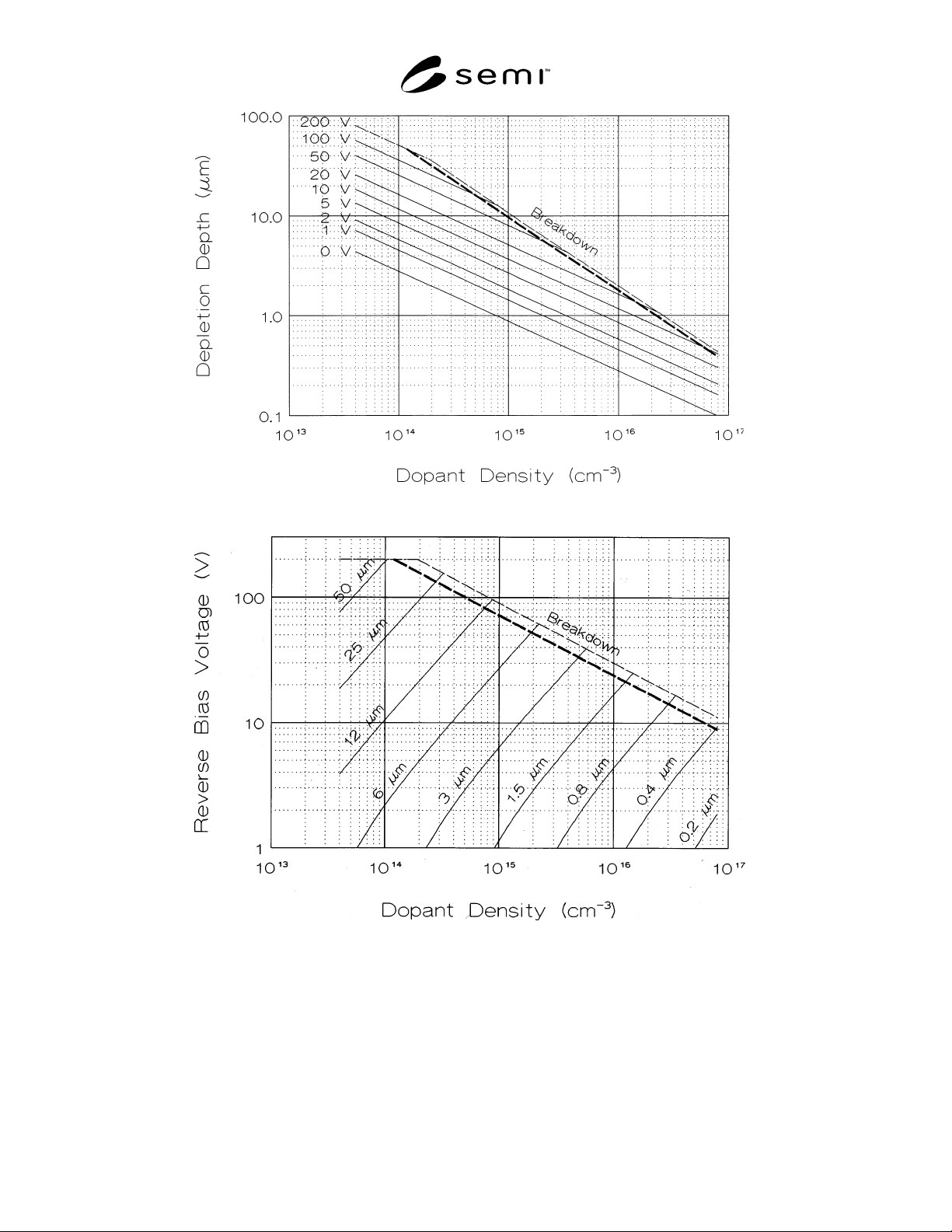
SEMI MF1392-1103 © SEMI 2003 2
(a) Depletion Depth as a Function of Dopant Density with Applied Reverse Bias Voltage as a Parameter.
(b) Applied Reverse Bias Voltage as a Function of Dopant Density with Depletion as a Parameter.
Note: The light dashed line represents the applied reverse bias voltage at which breakdown occurs in a
mercury-silicon contact; the heavy dashed line represents 80 % of this voltage, it is recommended that the
applied reverse bias voltage not exceed this value. The light chain-dot line represents the maximum
reverse bias voltage specified in this test method.
Figure 1
Relationship Between Depletion Depth, Applied Reverse Bias Voltage, and Dopant Density

SEMI MF1392-1103 © SEMI 2003 3
2.7 Warnings and precautionary notes regarding
potential safety hazards are provided throughout the
document.
NOTICE: This standard does not purport to address
safety issues, if any, associated with its use. It is the
responsibility of the user of this standard to establish
appropriate safety and health practices and determine
the applicability of regulatory or other limitations prior
to use.
3 Limitations
3.1 A poor Schottky contact, which is generally
indicated by an excessively high leakage current (see
Section 11.5) is the most common problem in
capacitance-voltage measurements made with mercury
probe instruments. It must be emphasized that the use
of a poor Schottky contact does not actually prevent a
carrier density determination but produces an
erroneous result.
3.2 Improper determination of the compensation
capacitance, C
comp
, (see Section 10.3) can cause
significant errors in the capacitance measurement. In
homogeneous material, improper zeroing or use of an
improper value for C
comp
results in an apparent
monotonic increase or decrease of carrier density with
distance from the Schottky barrier. In some fixtures,
inherently large stray capacitances exist; in such cases,
the value of C
comp
may depend both on the diameter of
the wafer and on the position of the wafer on the chuck.
If these dependencies are observed, they may be
reduced or eliminated by shielding the mercury probe
column. If shielding is not practical, probe calibration
procedures should be carried out with wafers of the
same diameter as the wafers being tested and care
should be taken to ensure that the geometry of wafer
and probe is the same during calibration and
measurement.
3.3 Alternating frequency test signals greater than 0.05
V rms may lead to errors in the measured capacitance.
3.4 Excessive series resistance in the capacitance
measurement circuit can cause significant errors in the
measured capacitance values. Series resistance values
greater than 1 kΩ have been reported to cause
measurement error in some cases.
4,5
The primary
source of excessive series resistance is generally a high-
resistance return contact; other possible sources are
bulk resistance in the wafer and wiring defects in the
4 Wiley, J. D., and Miller, G. L., “Series Resistance Effects in
Semiconductor CV Profiling,” IEEE Trans. Electron Devices ED-22,
265–272 (1975).
5 Schroder, D. K., Semiconductor Material and Device
Characterization (Wiley-Interscience, New York, 1990) Section
2.5.2.
mercury probe fixture or the test cables (see Section
11.4).
3.5 When exposed to air, a scum tends to form on the
exposed surface of the mercury used to form the
mercury probe contact. When freed from the surface,
this scum floats to the top of the mercury column. It is
necessary to make certain that the mercury that contacts
the wafer surface is clean by changing the mercury
periodically or by otherwise removing the scum from
the exposed surface.
3.6 A dirty or damaged capillary tube containing the
mercury column may also result in unstable
measurements (see Section 10.4.2.2).
3.7 If the reference wafer is not sufficiently uniform
throughout its thickness, the value of net carrier density,
N
ref
, determined by the four-point probe measurement
(see Section 8.4.3) may differ from the value of net
carrier density at the surface where the mercury probe
measurement is made. Use of erroneous values of N
ref
results in incorrect values for effective probe contact
area (see Section 10.3). Further, if the resistivity profile
of the reference wafer is not uniform near the surface,
an incorrect value of C
comp
may be obtained (see
Section 10.2). Incorrect values of probe contact area
and C
comp
result in incorrect values for the average net
carrier density of the test specimen.
4 Referenced Standards
4.1 SEMI Standards
SEMI C28 — Specifications and Guidelines for
Hydrofluoric Acid
SEMI C29 — Specifications and Guideline for 4.9%
Hydrofluoric Acid (10:1 v/v)
SEMI C30 — Specifications and Guidelines for
Hydrogen Peroxide
SEMI MF26 — Test Methods for Determining the
Orientation of a Semiconductive Single Crystal
SEMI MF42 — Test Methods for Conductivity Type of
Extrinsic Semiconducting Materials
SEMI MF81 — Test Method for Measuring Radial
Resistivity Variation on Silicon Wafers
SEMI MF84 — Test Method for Measuring Resistivity
of Silicon Wafers with an In-Line Four-Point Probe
SEMI MF672 — Test Method for Measuring
Resistivity Profiles Perpendicular to the Surface of a
Silicon Wafer Using a Spreading Resistance Probe
SEMI MF723 — Practice for Conversion Between
Resistivity and Dopant Density for Boron-Doped,
Phosphorus-Doped, and Arsenic-Doped Silicon